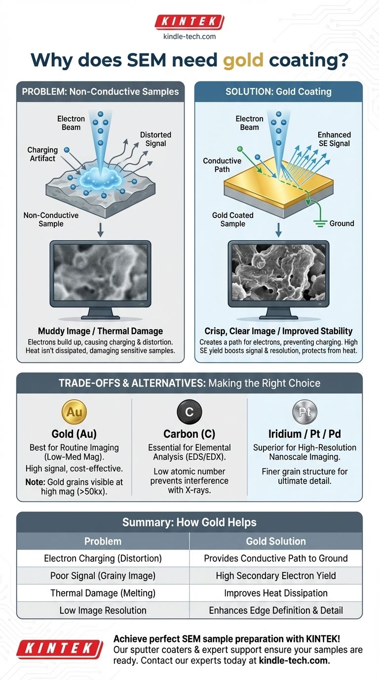
In short, a Scanning Electron Microscope (SEM) requires gold coating for non-conductive samples to prevent image distortion and improve image quality. The ultra-thin layer of gold makes the sample electrically conductive, providing a path for electrons to escape to ground, and its properties significantly enhance the signal used to create the final image.
The core issue is that SEMs use a beam of electrons to see a sample. If the sample isn't conductive, these electrons accumulate on the surface, creating electrical "charging" that severely degrades the image. Gold coating is the classic solution to make the sample visible to the electron beam.
The Fundamental Problem: Non-Conductive Samples in SEM
A Scanning Electron Microscope works by bombarding a sample with a focused beam of electrons and detecting the signals that bounce off. This process is fundamentally electrical, which creates major issues when the sample itself cannot conduct electricity.
The "Charging" Artifact
When the electron beam hits a non-conductive surface (like a polymer, ceramic, or biological specimen), the electrons have nowhere to go. They get stuck.
This buildup of negative charge on the surface, known as charging, deflects the incoming electron beam and distorts the signals leaving the sample. The result is a distorted, often unusably bright or shifting image.
Poor Signal Generation
The most important signal for SEM imaging is secondary electrons (SE), which are low-energy electrons ejected from the sample's surface atoms. This signal creates the detailed topographic image.
Many non-conductive materials are inherently poor emitters of secondary electrons. This leads to a low signal-to-noise ratio, resulting in a "muddy" or grainy image that lacks sharp detail.
Thermal Damage
The energy from the electron beam is deposited into the sample as heat. On a non-conductive sample, this heat cannot dissipate easily, which can lead to melting, warping, or complete destruction of delicate structures.
How Gold Coating Solves These Problems
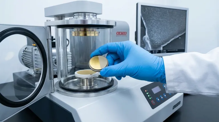
Applying an incredibly thin layer of metal—a process called sputter coating—directly counteracts these issues. Gold is a traditional and highly effective choice for this process.
Creating a Conductive Path
The primary function of the gold coating is to create a conductive path from the sample surface to the grounded SEM sample holder.
This path allows the excess electrons from the beam to flow away harmlessly, completely preventing the charging artifact and stabilizing the image.
Enhancing the Imaging Signal
Gold has a very high secondary electron yield. This means that when the primary electron beam strikes the gold-coated surface, it ejects a large number of secondary electrons.
This flood of signal dramatically increases the signal-to-noise ratio, producing the crisp, clear, and high-contrast images that SEM is known for.
Improving Stability and Resolution
By providing a path for thermal energy to escape, the coating increases thermal conduction and protects sensitive specimens from beam damage.
The coating also reduces how far the electron beam penetrates the sample. This improves edge resolution, making the boundaries and fine details of a structure appear much sharper.
Understanding the Trade-offs and Common Pitfalls
While gold is an excellent general-purpose coating, it is not always the best choice. Understanding its limitations is critical for accurate analysis.
The Gold Grain Structure
Sputter coating does not create a perfectly smooth film. It deposits the gold as a collection of nanoscale grains.
At low to medium magnifications, this isn't a problem. But at very high magnifications (typically above 50,000x), you may begin to image the texture of the gold coating itself, not the true surface of your sample. For true nanoscale imaging, finer-grained metals like Iridium or Platinum/Palladium are superior.
Obscuring Elemental Data
The gold coating completely covers the original sample. This makes it impossible to perform elemental analysis (such as Energy-Dispersive X-ray Spectroscopy, or EDS/EDX), as the detector will only see the signal from gold.
If your goal is to determine the chemical composition of your sample, you must use a different material. Carbon coating is the standard for elemental analysis because its low atomic number produces minimal interference with the X-ray signals from the underlying sample.
Making the Right Coating Choice
Your choice of coating must be driven by your analytical goal. There is no single "best" material for all applications.
- If your primary focus is routine imaging at low-to-medium magnification: Gold is the reliable, cost-effective, and high-signal choice.
- If your primary focus is elemental analysis (EDS/EDX): You must use carbon coating to get accurate compositional data from your sample.
- If your primary focus is very high-resolution imaging of nanostructures: A finer-grained (and more expensive) metal like Iridium or Platinum/Palladium is required to avoid imaging the coating's texture.
Ultimately, proper sample preparation is the foundation of good microscopy, and selecting the right coating is crucial for obtaining reliable and meaningful data.
Summary Table:
| Problem with Non-Conductive Samples | How Gold Coating Helps |
|---|---|
| Electron Charging (Image Distortion) | Provides a conductive path to ground |
| Poor Secondary Electron Signal | High secondary electron yield for crisp images |
| Thermal Damage (Beam Damage) | Improves heat dissipation |
| Low Image Resolution | Enhances edge definition and detail |
Achieve perfect SEM sample preparation with KINTEK!
Struggling with charging artifacts or poor image quality? Our sputter coaters and expert support ensure your non-conductive samples are prepared correctly for clear, reliable SEM imaging.
KINTEK specializes in lab equipment and consumables, serving all your laboratory needs. Let our expertise guide you to the best coating solution for your specific application.
Contact our experts today for a consultation and see the difference proper preparation makes!
Visual Guide
Related Products
- Electron Beam Evaporation Coating Gold Plating Tungsten Molybdenum Crucible for Evaporation
- Custom CVD Diamond Coating for Lab Applications
- HFCVD Machine System Equipment for Drawing Die Nano-Diamond Coating
- High Purity Gold Platinum Copper Iron Metal Sheets
People Also Ask
- What is e-beam evaporation? Achieve High-Purity Thin Film Deposition for Your Lab
- What is the current of e-beam evaporation? A Guide to High-Purity Thin Film Deposition
- How is an electron beam evaporator cooled during deposition? Essential Thermal Management for Stable Processes
- What is the voltage of e-beam evaporation? Achieve Precise Thin-Film Deposition
- What materials are used in electron beam evaporation? Master High-Purity Thin Film Deposition