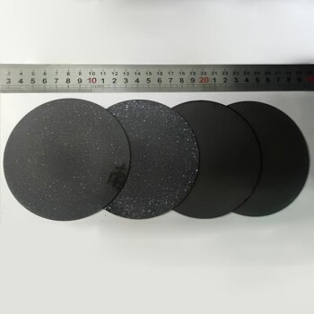
Introduction to Diamond as a Semiconductor Material
Significance of Large-Size Single-Crystal Diamonds
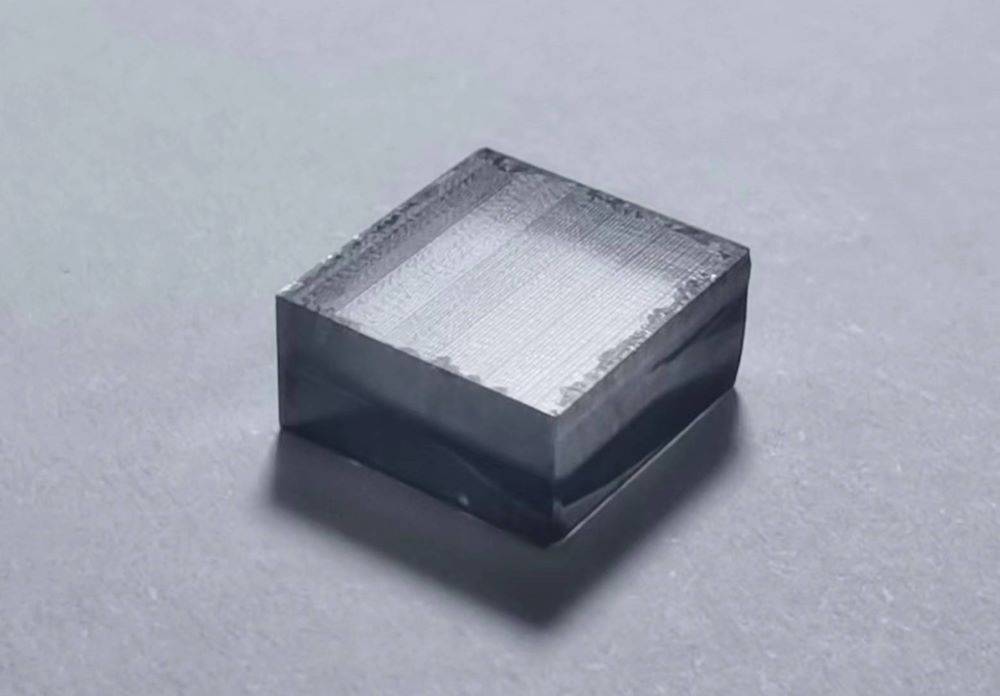
Large-size single-crystal diamonds hold immense potential for revolutionizing next-generation power electronics and optoelectronics devices. These materials offer exceptional properties such as high thermal conductivity, wide bandgap, and excellent mechanical strength, making them ideal for applications requiring high efficiency and reliability. However, the preparation of high-quality, large-area single-crystal diamond substrates remains a significant challenge.
The demand for larger diamond substrates is driven by the need for higher performance and integration density in electronic devices. Despite advancements in techniques like Microwave Plasma Chemical Vapor Deposition (MPCVD), achieving uniform growth over large areas with minimal defects is still an ongoing research area. The primary obstacles include controlling the dislocation density, managing thermal stresses, and ensuring homogeneity across the substrate.
Moreover, the scalability of these techniques is crucial for industrial applications. Current methods, such as single diamond growth and splicing growth, while promising, face limitations in producing inch-scale diamonds with the required quality. Heterogeneous epitaxial growth, though easier to scale, introduces higher dislocation densities due to lattice and thermal mismatches with the substrate.
In summary, while large-size single-crystal diamonds are poised to transform various industries, significant technological advancements are necessary to overcome the current limitations in their production.
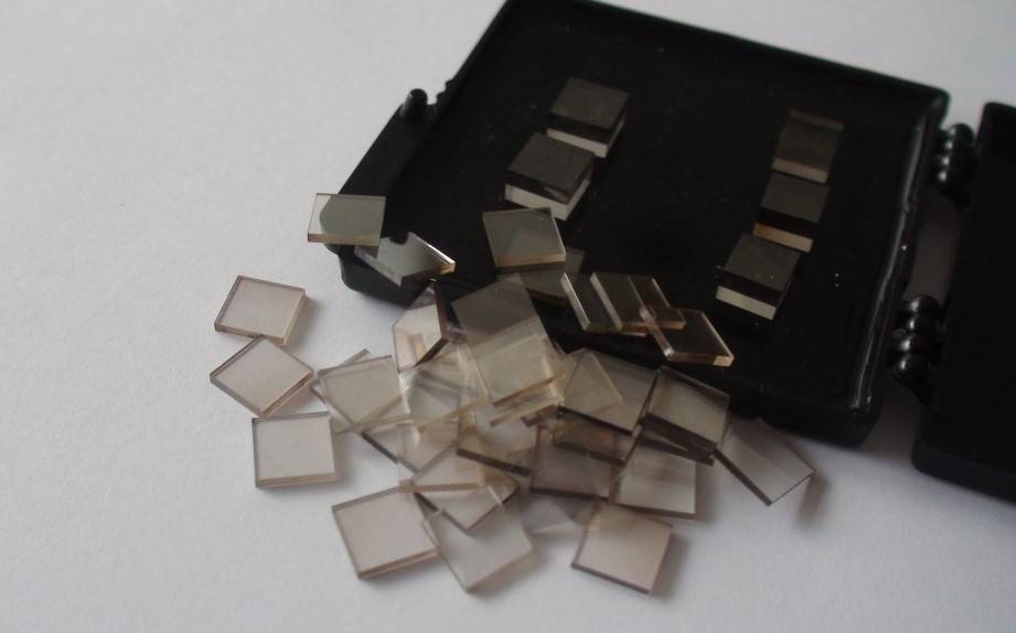
Technical Solutions for Large-Size Diamond Preparation
Single Diamond Growth
Single diamond growth techniques are renowned for producing high-quality crystals characterized by a low dislocation density. However, these methods encounter significant obstacles when attempting to achieve diamonds of inch-scale dimensions. The intricate process involves precise control over factors such as temperature, pressure, and the presence of impurities like nitrogen.
Historically, the first synthetic gem-quality diamonds were produced in the early 1970s, initially yielding stones of approximately 5 mm in size. These early successes utilized a pyrophyllite tube seeded with diamond fragments, and the growth process was meticulously controlled to ensure the stability necessary for high-quality crystal formation. Over time, advancements have been made, such as replacing graphite with diamond grit to enhance shape control, but the fundamental challenges remain.
One of the primary issues is the trade-off between growth rate and crystal quality. While nitrogen addition can accelerate the growth process, it introduces impurities that compromise the diamond's purity, particularly for applications requiring electronic-grade materials. Conversely, lower growth temperatures and reduced methane content can enhance crystal quality by minimizing dislocations and improving surface characteristics, but these parameters significantly reduce the growth rate.
| Growth Parameter | Impact on Crystal Quality | Impact on Growth Rate |
|---|---|---|
| Nitrogen Addition | Introduces impurities | Increases growth rate |
| Low Growth Temperature | Low dislocation density | Reduces growth rate |
| Reduced Methane Content | High-quality surface | Reduces growth rate |
Despite these advancements, achieving the ideal balance of high growth rate, low dislocation density, and a flat surface remains an ongoing challenge. The pursuit of inch-scale diamonds continues to drive research and development, with ongoing efforts focused on optimizing these parameters to unlock the full potential of single diamond growth techniques.
Splicing Growth Technique
The splicing growth technique represents a significant advancement in the production of large-size diamonds, enabling rapid fabrication of sizable crystals. However, this method is not without its challenges, particularly concerning the formation of dislocations and the buildup of stresses at the splice joints.
Dislocations, which are line defects in the crystal structure, often arise at the interfaces where different diamond segments are joined together. These defects can severely compromise the mechanical and electronic properties of the diamond, limiting its potential applications in high-performance devices. Additionally, the stresses generated at these splice joints can lead to the formation of cracks or other structural anomalies, further degrading the quality of the diamond.
To mitigate these issues, researchers are exploring various strategies, such as optimizing the alignment and bonding processes during splicing. Advanced characterization techniques, including high-resolution microscopy and X-ray diffraction, are also being employed to monitor and analyze the structural integrity of the diamond at the splice points. These efforts aim to enhance the overall quality and reliability of large-size diamonds produced through the splicing growth technique, paving the way for more widespread adoption in advanced semiconductor applications.
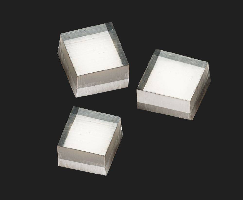
Heterogeneous Epitaxial Growth
Heterogeneous epitaxial growth of diamond offers a promising avenue for achieving large-size diamond wafers, drawing parallels from the advancements in other semiconductors. This technique involves the deposition of diamond layers on dissimilar substrates, which has been a focal point of early research efforts. Notably, in 1996, Ohtsuka et al. successfully fabricated a heteroepitaxial diamond layer on an Ir(001)/MgO(001) substrate, marking a significant milestone. Since then, the technology has evolved, with single-crystal iridium films being grown on various oxides such as Al₂O₃, SrTiO₃, and MgO.
However, the adhesion of diamond/Ir layers on these substrates presents a significant challenge due to substantial mismatches in thermal expansion coefficients. Bauer and colleagues calculated in 2005 the thermal stresses arising from cooldown after deposition at 700°C, revealing compressive stress values of –4.05 GPa on Al₂O₃, –6.44 GPa on SrTiO₃, and –8.3 GPa on MgO. In contrast, silicon exhibited the lowest stress at –0.68 GPa. Additionally, Yttria-Stabilized-Zirconia (YSZ) films have emerged as the optimal layer for depositing single-crystalline (100) oriented Ir buffer layers, leading to a promising heteroepitaxial film combination: Silicon/YSZ/Ir/diamond.
Despite these advancements, the inherent lattice and thermal mismatches with the substrate result in a higher dislocation density, which remains a critical issue. This dislocation density is a consequence of the significant differences in lattice constants and thermal expansion coefficients between the diamond and the substrate materials. Consequently, while heterogeneous epitaxial growth facilitates the production of large-size diamonds, it also necessitates ongoing research to mitigate these structural defects and enhance the quality of the resulting diamond films.
Research and Development Highlights
Lateral Epitaxial Overgrowth (LEO)
Lateral Epitaxial Overgrowth (LEO) represents a pioneering technique in the realm of single-crystal diamond synthesis, particularly aimed at overcoming the limitations associated with the growth of large-size diamonds. This method, as demonstrated by researchers at Shandong University, involves the strategic bridging of multiple seed crystals into a cohesive whole. By doing so, LEO not only facilitates the creation of larger diamond structures but also mitigates the dislocation density and stress concentrations typically found at the junctions of spliced crystals.
The innovation behind LEO lies in its ability to harness the inherent properties of diamond crystals to grow laterally, thereby expanding the overall crystal size without the need for additional seeding. This approach is particularly advantageous in the context of Microwave Plasma Chemical Vapor Deposition (MPCVD), where the controlled environment allows for precise manipulation of growth parameters. The result is a more uniform and structurally robust diamond, which is critical for applications in next-generation power electronics and optoelectronics.
Moreover, LEO's potential to significantly reduce dislocation density stands as a testament to its efficacy in addressing one of the primary challenges in diamond synthesis. This reduction in dislocations not only enhances the mechanical integrity of the diamond but also improves its optical and electrical properties, making it a superior material for high-performance device fabrication.
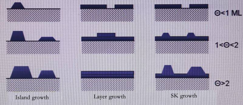
In essence, LEO embodies a significant stride forward in the quest to produce large-size, high-quality single-crystal diamonds, offering a promising solution to the intricate challenges of diamond growth and positioning it as a cornerstone in the future of semiconductor materials.
Heterogeneous Epitaxial Growth Achievements
The SCHRECK team at the University of Augsburg has made significant strides in the field of heterogeneous epitaxial growth, particularly in the realm of large-size single-crystal diamond preparation. Their most notable achievement to date is the successful growth of a 92 mm diameter diamond, a feat that underscores the potential of this technique to produce substantial diamond crystals. This achievement is not merely a demonstration of technical prowess but also a testament to the scalability of heterogeneous epitaxial growth methods.
The growth of such a large diamond crystal is particularly noteworthy given the inherent challenges associated with heterogeneous epitaxial growth, primarily the higher dislocation density due to lattice and thermal mismatches with the substrate. The SCHRECK team's success suggests that with careful optimization of growth parameters and substrate selection, these challenges can be mitigated, paving the way for the production of even larger and higher-quality diamonds.
Moreover, this advancement has broader implications for the semiconductor industry, where large-size single-crystal diamonds are highly sought after for their exceptional properties in power electronics and optoelectronics devices. The ability to consistently produce such diamonds could revolutionize the manufacturing of next-generation devices, offering enhanced performance and reliability.
Challenges and Future Directions
Reducing Dislocation Density
Reducing dislocation density is crucial for achieving high-quality, large-size single-crystal diamonds, which are essential for advanced semiconductor applications. Two primary methods have emerged as key strategies in this endeavor: lateral epitaxial growth and dislocation annihilation techniques.
Lateral Epitaxial Growth (LEO)
Lateral epitaxial overgrowth (LEO) is a sophisticated approach that involves the growth of diamond layers over pre-existing seed crystals. This technique, pioneered by researchers at Shandong University, allows for the bridging of multiple seed crystals into a cohesive whole. By strategically controlling the growth conditions, LEO can significantly reduce the dislocation density by enabling the formation of a continuous crystal lattice over larger areas. This method is particularly effective in mitigating the effects of lattice mismatches and thermal stresses, which are common challenges in diamond growth processes.
Dislocation Annihilation Techniques
Dislocation annihilation techniques focus on the elimination of dislocations, which are linear defects in the crystal lattice that can degrade the material's properties. These techniques often involve the application of external stress or heat to induce the movement and subsequent annihilation of dislocations. For instance, the application of a high-temperature annealing process can facilitate the migration of dislocations to the surface of the crystal, where they can be eliminated. Additionally, the use of selective epitaxial growth can create regions of the crystal with fewer dislocations, further enhancing the overall quality of the diamond.
Both lateral epitaxial growth and dislocation annihilation techniques offer promising avenues for overcoming the challenges associated with dislocation density in large-size single-crystal diamond preparation. As research continues to advance, these methods are expected to play a pivotal role in the development of next-generation semiconductor materials.
Impurity Control
The control of impurities such as nitrogen and silicon is a critical aspect of preparing high-quality, large-size single-crystal diamonds. The industry has proposed a counterintuitive method to mitigate these impurities: the addition of oxygen to the growth environment. While this approach is widely practiced, the underlying mechanisms are not yet fully understood.
Studies suggest that oxygen interacts with nitrogen and silicon, forming volatile compounds that can be easily removed from the deposition chamber. This process not only reduces the concentration of these impurities in the growing diamond but also enhances the overall quality of the crystal. However, the exact chemical reactions and kinetic processes involved remain subjects of ongoing research.
| Impurity | Effect on Diamond Quality | Proposed Mitigation Method |
|---|---|---|
| Nitrogen | Increases yellow coloration, reduces thermal conductivity | Addition of oxygen to form volatile NOx |
| Silicon | Forms SiC, which can degrade diamond properties | Oxidation to form volatile SiO2 |
Further research is needed to elucidate the detailed mechanisms and optimize the conditions for oxygen addition. Understanding these processes could lead to more effective impurity control strategies, ultimately aiding in the production of larger, higher-quality single-crystal diamonds.
Related Products
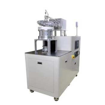
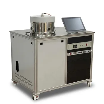
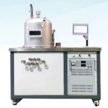
- Microwave Plasma Chemical Vapor Deposition MPCVD Machine System Reactor for Lab and Diamond Growth
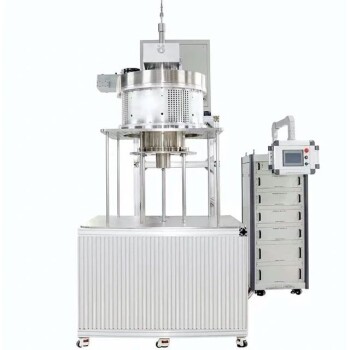
- 915MHz MPCVD Diamond Machine Microwave Plasma Chemical Vapor Deposition System Reactor
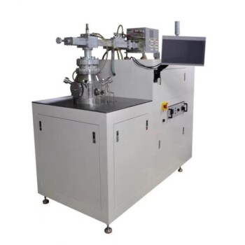
- Cylindrical Resonator MPCVD Machine System Reactor for Microwave Plasma Chemical Vapor Deposition and Lab Diamond Growth
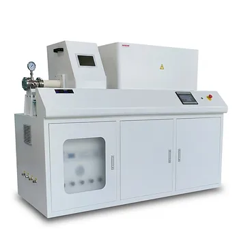
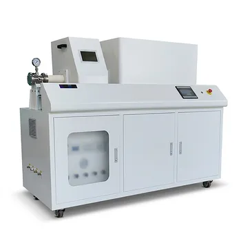
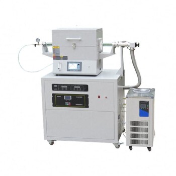
- Multi Heating Zones CVD Tube Furnace Machine Chemical Vapor Deposition Chamber System Equipment
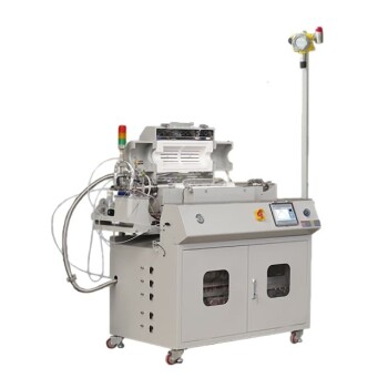
- Chemical Vapor Deposition CVD Equipment System Chamber Slide PECVD Tube Furnace with Liquid Gasifier PECVD Machine
Related Articles
- How to Achieve High Quality Single-Crystal Diamond with MPCVD
- A Comprehensive Guide to MPCVD: Diamond Synthesis and Applications
- MPCVD Cultured Diamond Revolutionizes the Industry
- Understanding MPCVD: A Comprehensive Guide to Microwave Plasma Chemical Vapor Deposition
- The Process of Fabricating a CVD Diamond By MPCVD Machine

