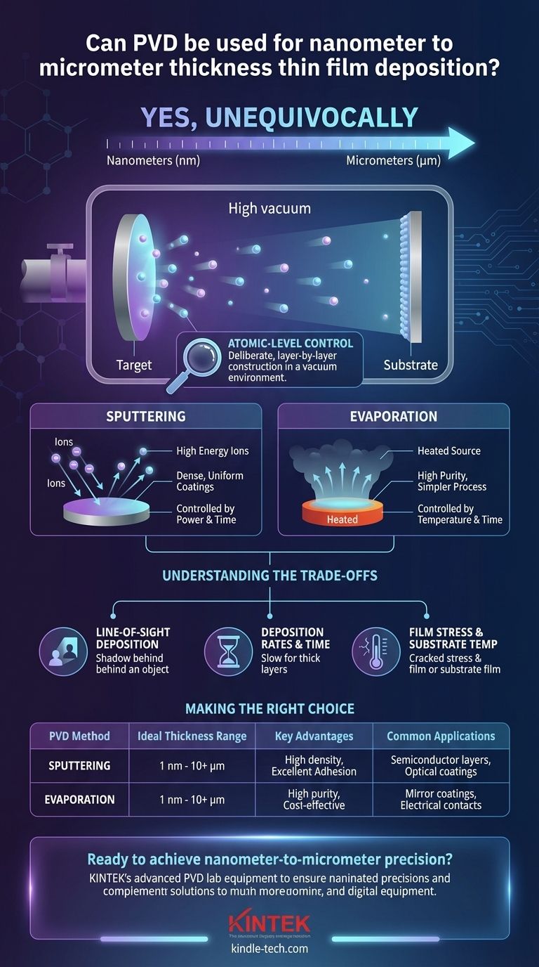
Yes, unequivocally. Physical Vapor Deposition (PVD) is not just capable of depositing thin films in the nanometer to micrometer range; it is one of the cornerstone technologies for doing so with exceptional precision. The process operates in a vacuum, transforming solid material into atomic particles that are then deposited onto a substrate, allowing for meticulous control over the final film thickness and quality.
The core value of PVD is not just its ability to create thin films, but its atomic-level control. By manipulating process parameters within a vacuum, PVD allows for the deliberate, layer-by-layer construction of materials, making it ideal for applications demanding precision from a few nanometers to several micrometers.

How PVD Achieves Nanometer-to-Micrometer Precision
The precision of PVD is not accidental; it is a direct result of the physics governing the process. Several key factors work together to enable this fine control.
The Critical Role of the Vacuum Environment
All PVD processes occur under a high vacuum. This is fundamental to its success.
A vacuum removes atmospheric gases that could otherwise react with the deposition material or interfere with the particles' path to the substrate. This pristine environment ensures film purity and allows for a direct, predictable deposition.
Atomic-Level Deposition
PVD works by depositing material atom by atom or in very small clusters of atoms. This is fundamentally different from processes like painting or plating, which involve much larger particles or continuous fluid flow.
This atomic-scale buildup is the source of PVD's precision. By controlling the rate at which these atoms arrive at the substrate surface, you directly control the growth rate of the film.
Key PVD Methods and Their Control
The most common PVD methods, sputtering and evaporation, both leverage this atomic-level control.
Sputtering uses high-energy ions to bombard a target material, ejecting atoms that then travel to and coat the substrate. The thickness is precisely controlled by managing the power applied to the target and the total deposition time. This method is known for producing very dense, uniform, and highly adherent films.
Evaporation involves heating a material in the vacuum until it turns into a vapor. This vapor then travels to the cooler substrate and condenses on its surface, forming the film. Control is achieved by regulating the temperature of the source material and the duration of the process.
Understanding the Trade-offs and Limitations
While powerful, PVD is not a universal solution. Understanding its limitations is key to using it effectively.
Line-of-Sight Deposition
Most PVD processes are "line-of-sight," meaning the coating material travels in a straight line from the source to the substrate.
This makes it difficult to uniformly coat complex 3D shapes, sharp corners, or the inside of deep trenches. The parts that are "shadowed" from the source will receive little to no coating.
Deposition Rates and Time
Achieving nanometer precision takes time. While perfect for thin films, PVD can be a relatively slow process compared to chemical methods if the goal is to deposit very thick layers (e.g., over 50-100 micrometers).
The need for high-vacuum equipment also makes the initial capital investment significant.
Film Stress and Substrate Temperature
The deposition process can induce internal stresses within the thin film, which can cause cracking or delamination if not properly managed.
Additionally, some PVD processes require heating the substrate to achieve desired film properties, which may not be suitable for temperature-sensitive materials like certain plastics.
Making the Right Choice for Your Application
Selecting the right deposition technique depends entirely on your end goal. PVD offers unparalleled control within its ideal thickness range.
- If your primary focus is ultimate precision and film density (e.g., optical filters, semiconductor layers): Sputtering is the superior choice due to its high energy, which creates dense and uniform coatings.
- If your primary focus is coating a simple surface with a pure metal (e.g., mirror coatings, electrical contacts): Thermal evaporation is often a more cost-effective and simpler PVD method that provides excellent results.
- If your primary focus is coating a highly complex 3D object uniformly: You should evaluate whether PVD is the right fit or if an alternative like Atomic Layer Deposition (ALD) or Chemical Vapor Deposition (CVD) is necessary.
Physical Vapor Deposition remains a foundational and indispensable tool for engineering materials at the micro and nano scales.
Summary Table:
| PVD Method | Ideal Thickness Range | Key Advantages | Common Applications |
|---|---|---|---|
| Sputtering | 1 nm - 10+ µm | High density, excellent adhesion, uniform coatings | Semiconductor layers, optical coatings |
| Evaporation | 1 nm - 10+ µm | High purity, simpler process, cost-effective | Mirror coatings, electrical contacts |
Ready to achieve nanometer-to-micrometer precision in your thin film applications? KINTEK specializes in providing advanced PVD lab equipment and consumables tailored to your laboratory's specific needs. Our expertise ensures you get the right solution for superior film density, uniformity, and adhesion. Contact our experts today to discuss how our PVD solutions can enhance your research and development!
Visual Guide
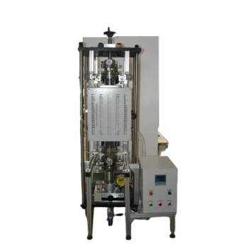
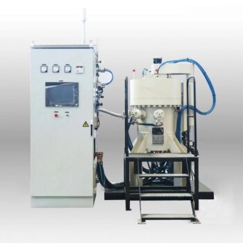
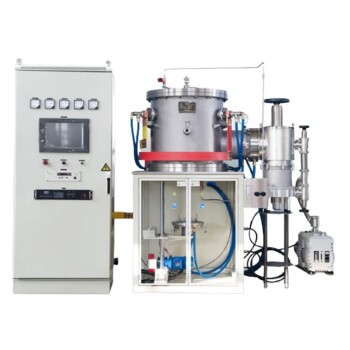
Related Products
- RF PECVD System Radio Frequency Plasma-Enhanced Chemical Vapor Deposition RF PECVD
- Split Chamber CVD Tube Furnace with Vacuum Station Chemical Vapor Deposition System Equipment Machine
- Chemical Vapor Deposition CVD Equipment System Chamber Slide PECVD Tube Furnace with Liquid Gasifier PECVD Machine
- VHP Sterilization Equipment Hydrogen Peroxide H2O2 Space Sterilizer
- Vacuum Hot Press Furnace Heated Vacuum Press Machine Tube Furnace
People Also Ask
- Why does PECVD commonly use RF power input? For Precise Low-Temperature Thin Film Deposition
- How does RF power create plasma? Achieve Stable, High-Density Plasma for Your Applications
- Why is PECVD environment friendly? Understanding the Eco-Friendly Benefits of Plasma-Enhanced Coating
- How are PECVD and CVD different? A Guide to Choosing the Right Thin-Film Deposition Process
- What is plasma activated chemical vapour deposition method? A Low-Temperature Solution for Advanced Coatings