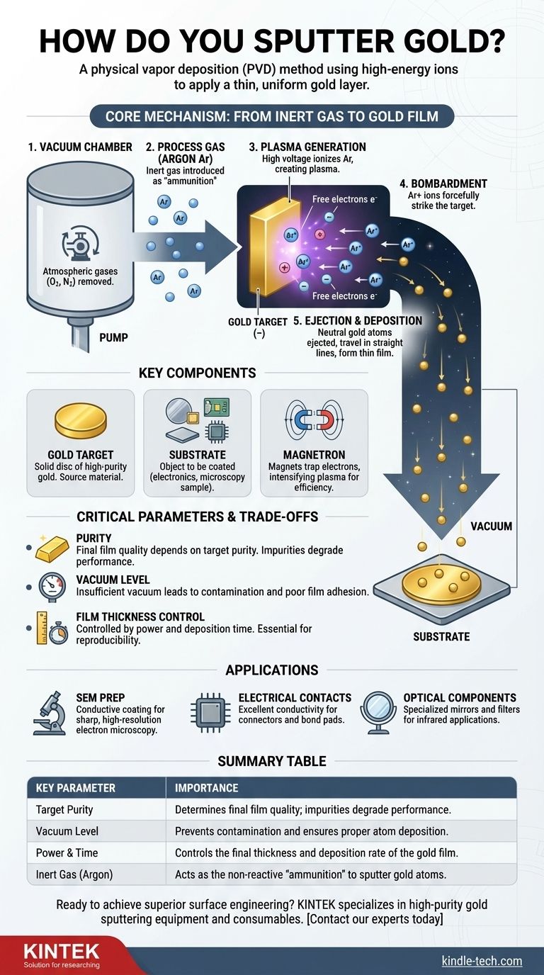
Sputtering gold is a physical vapor deposition (PVD) method used to apply an exceptionally thin and uniform layer of gold onto a surface. It does not involve a chemical reaction. Instead, it uses high-energy ions from an inert gas, like argon, to physically knock gold atoms off a solid source material, known as a target. These dislodged gold atoms then travel through a vacuum and deposit onto the desired object, or substrate, forming the coating.
At its core, gold sputtering is a highly controlled, atomic-scale sandblasting process. It uses energized gas ions to chip individual atoms from a pure gold source, which then settle as a consistent thin film on a target surface within a vacuum chamber.
The Core Mechanism: From Inert Gas to Gold Film
Understanding the sputtering process requires breaking it down into a sequence of physical events that occur under precisely controlled conditions.
Creating the Vacuum Environment
The entire process must happen in a high-vacuum chamber. This initial step is critical because it removes atmospheric gases like oxygen and nitrogen, which could otherwise react with the gold or interfere with the deposition, contaminating the final film.
Introducing the Process Gas
Once a vacuum is established, a small, measured amount of a high-purity inert gas, most commonly argon (Ar), is backfilled into the chamber. This gas will not chemically react with the gold but will serve as the "ammunition" for the sputtering process.
Generating the Plasma
A strong negative electrical voltage is applied to the solid gold target. This high voltage ionizes the argon gas atoms by stripping them of electrons, creating a mixture of positively charged argon ions (Ar+) and free electrons. This energized, glowing state of matter is known as a plasma.
The Bombardment Phase
The positively charged argon ions are forcefully accelerated toward the negatively charged gold target, much like opposite poles of a magnet attract. They collide with the surface of the gold target with significant kinetic energy.
Ejection and Deposition
This high-energy impact is the "sputtering" event. The momentum from the argon ion is transferred to the gold atoms on the surface, giving them enough energy to be knocked loose or "sputtered" from the target. These ejected, neutral gold atoms then travel in straight lines until they strike a surface—including your substrate—where they condense to form a thin, even film.
Key Components of a Sputtering System
Several key components work in concert to make this process possible.
The Gold Target
This is the source material for the coating. It is a solid disc or plate of extremely pure gold. The purity is paramount, as any impurities in the target will be transferred into the final film, potentially altering its electrical or optical properties.
The Substrate
This is simply the object or material you intend to coat with gold. It can range from a silicon wafer for electronics to a biological sample for microscopy.
The Magnetron
Modern sputtering systems often place magnets behind the target. This device, known as a magnetron, uses magnetic fields to trap the free electrons from the plasma near the surface of the target. This intensifies the ionization of the argon gas, making the sputtering process much more efficient and allowing it to run at lower pressures.
Understanding the Trade-offs and Critical Parameters
While powerful, the sputtering process is not without its complexities. Achieving a high-quality result depends on careful control over several variables.
The Importance of Purity
The final film is only as pure as its source. Using a lower-purity gold target can introduce contaminants that degrade electrical conductivity, increase contact resistance, or alter optical properties. This is a critical factor for high-performance applications.
The Role of Vacuum Level
A "leaky" or insufficient vacuum is a common failure point. If the vacuum is poor, residual atmospheric atoms will collide with the sputtered gold atoms during their flight, potentially causing them to react or scatter. This leads to a contaminated, less dense, and poorly adhered film.
Control Over Film Thickness
The thickness of the deposited gold layer is controlled by two main factors: the power applied to the target and the deposition time. Higher power results in a more intense ion bombardment and a faster deposition rate. Precise control over these parameters is essential for creating films with reproducible and specific thicknesses.
How to Apply This to Your Project
Gold sputtering is chosen for specific applications where its unique properties are essential.
- If your primary focus is preparing non-conductive samples for electron microscopy (SEM): Sputtering a thin gold coating provides a conductive path to ground the sample, preventing charge buildup and enabling sharp, high-resolution imaging.
- If your primary focus is creating high-reliability electrical contacts: Sputtered gold is ideal for connectors, bond pads, and electrodes in electronics due to its excellent conductivity and superior resistance to corrosion and oxidation.
- If your primary focus is manufacturing optical components: A precisely controlled layer of sputtered gold can be used to create specialized mirrors and filters, particularly for infrared applications.
Ultimately, gold sputtering is a precise and versatile method for engineering surfaces at the atomic level, delivering performance critical for science and technology.
Summary Table:
| Key Parameter | Importance |
|---|---|
| Target Purity | Determines final film quality; impurities degrade performance. |
| Vacuum Level | Prevents contamination and ensures proper atom deposition. |
| Power & Time | Controls the final thickness and deposition rate of the gold film. |
| Inert Gas (Argon) | Acts as the non-reactive "ammunition" to sputter gold atoms. |
Ready to achieve superior surface engineering with gold sputtering? KINTEK specializes in high-purity lab equipment and consumables, including gold sputtering targets and systems. Whether you are preparing samples for SEM analysis, creating reliable electrical contacts, or developing optical components, our solutions ensure precise, contamination-free results. Contact our experts today to discuss how we can support your laboratory's specific coating needs!
Visual Guide
Related Products
People Also Ask
- What is e-beam evaporation? Achieve High-Purity Thin Film Deposition for Your Lab
- What are the applications of e-beam evaporation? Achieve High-Purity Coatings for Optics & Electronics
- How is an electron beam evaporator cooled during deposition? Essential Thermal Management for Stable Processes
- What materials are used in electron beam evaporation? Master High-Purity Thin Film Deposition
- What is the container that holds the metal source material called in e-beam evaporation? Ensure Purity and Quality in Your Thin-Film Deposition
