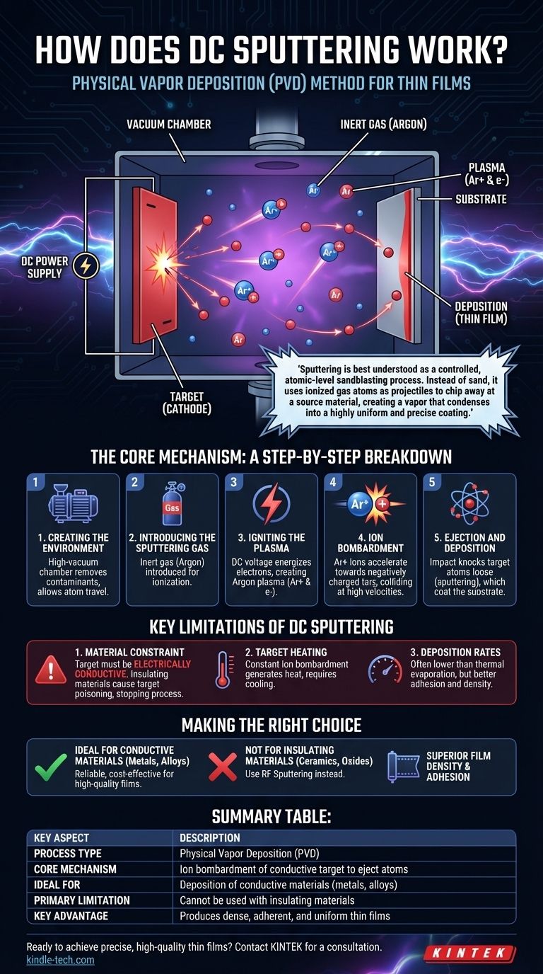
At its core, DC sputtering is a physical vapor deposition (PVD) method that uses an energized gas to physically knock atoms off a source material and deposit them onto another object as a thin film. The process works by creating a high-voltage electric field between the source material (the target) and the object to be coated (the substrate) within a vacuum chamber filled with an inert gas, typically Argon. This field ionizes the gas, and the resulting ions accelerate into the target, dislodging atoms that then coat the substrate.
Sputtering is best understood as a controlled, atomic-level sandblasting process. Instead of sand, it uses ionized gas atoms as projectiles to chip away at a source material, creating a vapor that condenses into a highly uniform and precise coating.
The Core Mechanism: A Step-by-Step Breakdown
To truly understand how DC sputtering works, it's best to visualize it as a sequence of events occurring inside a specialized vacuum chamber. Each step is critical for building the final thin film with the desired properties.
Step 1: Creating the Environment
The entire process begins by placing the target (the material to be deposited) and the substrate (the object to be coated) into a high-vacuum chamber.
The vacuum is essential for two reasons. First, it removes air and other contaminants that could react with the sputtered material and ruin the film. Second, it allows the sputtered atoms to travel from the target to the substrate with minimal collisions.
Step 2: Introducing the Sputtering Gas
Once a vacuum is established, a small, precisely controlled amount of an inert gas, almost always Argon, is introduced into the chamber.
Argon is used because it is chemically non-reactive and has a suitable atomic mass for effectively dislodging atoms from most target materials.
Step 3: Igniting the Plasma
A high-voltage Direct Current (DC) power supply is activated. The target is connected to the negative terminal (making it the cathode), and the chamber or a separate anode is connected to the positive terminal.
This strong electric field energizes free electrons within the chamber. These high-energy electrons collide with the neutral Argon gas atoms, knocking electrons off them and creating positively charged Argon ions (Ar+) and more free electrons. This self-sustaining cloud of ions and electrons is known as a plasma.
Step 4: Ion Bombardment
The positively charged Argon ions (Ar+) are now strongly accelerated by the electric field towards the negatively charged target.
They collide with the target surface at very high velocities, transferring a significant amount of kinetic energy and momentum.
Step 5: Ejection and Deposition
The impact from the Argon ions is forceful enough to physically knock atoms loose from the target material. This ejection of atoms is the "sputtering" effect.
These sputtered atoms travel through the vacuum chamber and land on the substrate, gradually building up, atom by atom, to form a thin, uniform film.
Key Limitations of the DC Sputtering Process
While highly effective, the DC (Direct Current) method has specific constraints that are critical to understand. Its primary limitation dictates the type of materials it can be used for.
The Material Constraint
The single biggest limitation of DC sputtering is that the target material must be electrically conductive.
Because a constant negative voltage must be maintained on the target, an insulating or non-conductive material would cause a buildup of positive charge from the impacting ions. This effect, known as "target poisoning," quickly neutralizes the negative bias and extinguishes the plasma, stopping the sputtering process entirely.
Target Heating
The constant bombardment of ions generates a tremendous amount of heat in the target. Effective cooling systems are mandatory to prevent the target from melting, warping, or changing its material properties.
Deposition Rates
Compared to some thermal evaporation processes, DC sputtering can have lower deposition rates. However, the resulting films often have superior adhesion and density.
Making the Right Choice for Your Goal
Understanding the mechanism reveals when DC sputtering is the ideal choice for thin-film deposition and when an alternative is required.
- If your primary focus is depositing metals, alloys, or other conductive materials: DC sputtering is an extremely reliable, cost-effective, and widely used method for producing high-quality films.
- If your primary focus is depositing ceramics, oxides, or other insulating materials: DC sputtering will not work; you must use a technique like Radio Frequency (RF) Sputtering, which uses an AC field to avoid charge buildup.
- If your primary focus is achieving superior film density and adhesion: Sputtering in general is an excellent choice, as the high kinetic energy of the deposited atoms creates denser and more adherent films than many other methods.
Ultimately, mastering this process is about harnessing a controlled atomic collision to build high-performance materials from the ground up.
Summary Table:
| Key Aspect | Description |
|---|---|
| Process Type | Physical Vapor Deposition (PVD) |
| Core Mechanism | Ion bombardment of a conductive target to eject atoms |
| Ideal For | Deposition of conductive materials (metals, alloys) |
| Primary Limitation | Cannot be used with insulating materials (ceramics, oxides) |
| Key Advantage | Produces dense, adherent, and uniform thin films |
Ready to achieve precise, high-quality thin films for your laboratory?
DC sputtering is a cornerstone technique for depositing conductive materials, but choosing the right equipment is critical for success. KINTEK specializes in providing reliable lab equipment and consumables tailored to your research and production needs.
Whether you are working with metals, alloys, or exploring other deposition methods, our expertise can help you optimize your process. Contact us today to discuss how our solutions can enhance your lab's capabilities and ensure your projects are a success.
Contact KINTEK for a consultation
Visual Guide
Related Products
- Spark Plasma Sintering Furnace SPS Furnace
- Circulating Water Vacuum Pump for Laboratory and Industrial Use
- Vacuum Induction Melting Spinning System Arc Melting Furnace
- Multi Heating Zones CVD Tube Furnace Machine Chemical Vapor Deposition Chamber System Equipment
People Also Ask
- What is the mechanism of SPS process? A Deep Dive into Rapid, Low-Temperature Sintering
- What are the fundamentals of spark plasma sintering process? Unlock Rapid, High-Performance Material Consolidation
- What technical advantages does a Spark Plasma Sintering (SPS) furnace offer for LZP ceramics? Enhance Ionic Conductivity
- Why are Spark Plasma Sintering (SPS) furnaces or hot presses utilized in the preparation of Li3PS4 solid electrolytes?
- What is the pressure for spark plasma sintering? A Guide to Optimizing SPS Parameters


