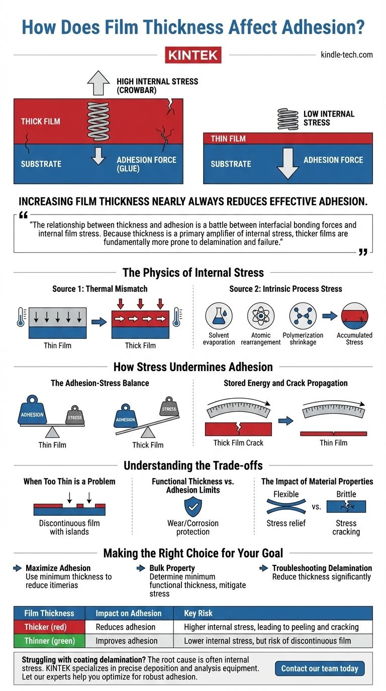
In nearly all cases, increasing film thickness reduces effective adhesion. While it may seem counterintuitive, thicker films generate higher internal stress, which works directly against the bonding forces holding the film to the substrate. This internal stress is the primary reason why thick coatings are more prone to peeling, cracking, and delamination.
The relationship between thickness and adhesion is a battle between interfacial bonding forces and internal film stress. Because thickness is a primary amplifier of internal stress, thicker films are fundamentally more prone to delamination and failure.
The Physics of Internal Stress
To understand the role of thickness, you must first understand internal stress. This is the mechanical stress that exists within a film even with no external forces applied.
What is Internal Stress?
Internal stress is a force within the film's material that is constantly pulling on itself and, critically, on the bond it has with the surface underneath (the substrate).
If this internal pulling force becomes greater than the adhesion force, the film will fail.
Source 1: Thermal Mismatch
Most films are applied at a high temperature and then cool to room temperature. The film and the substrate almost always have different rates of thermal expansion (Coefficient of Thermal Expansion, or CTE).
As the system cools, one material tries to shrink more than the other. This mismatch creates immense stress. A thicker film represents a larger volume of material trying to contract, which generates a proportionally larger total force.
Source 2: Intrinsic Process Stress
Stress can also be built into the film during the deposition or curing process itself.
This can come from solvent evaporation in paints, atomic rearrangement in vacuum deposition, or polymerization shrinkage in epoxies. Again, the more material you have (a thicker film), the more total shrinkage and stress you accumulate.
How Stress Undermines Adhesion
Internal stress does not reduce the chemical bonding at the interface, but it actively works to break that bond.
The Adhesion-Stress Balance
Think of adhesion as the "glue" holding the film down. Think of internal stress as a built-in "crowbar" trying to pry the film up.
A thin film might have a very small crowbar that is easily resisted by the glue. A thick film has a much larger, more powerful crowbar that can easily overcome the same amount of glue.
Stored Energy and Crack Propagation
A thicker film can store more elastic energy, much like a thicker bent ruler stores more energy than a thin one.
If a tiny defect or crack forms (often at an edge), this high stored energy has an outlet. It releases rapidly, driving the crack forward and causing catastrophic delamination of the film. A thin film has less stored energy and is less likely to fuel this kind of failure.
Understanding the Trade-offs
While thinner is generally better for adhesion, there are practical limits and considerations.
When Too Thin is a Problem
Extremely thin films (in the nanometer range) can be discontinuous, forming isolated islands instead of a coherent layer. This results in poor adhesion and fails to provide the film's intended function, such as being a barrier layer.
You must have enough thickness to form a continuous film before the principle of "thinner is better" truly applies.
Functional Thickness vs. Adhesion Limits
Many films are thick for a reason—to provide wear resistance, corrosion protection, or specific optical properties.
In these cases, you cannot simply make the film thinner. The challenge becomes managing the stress in a thick film through other means, such as material selection, process control, or adding intermediate stress-relief layers.
The Impact of Material Properties
The properties of the film itself are critical. A flexible, ductile film may be able to relieve stress through slight deformation, allowing it to be applied thicker than a rigid, brittle material.
Brittle materials like ceramics are highly susceptible to stress-related adhesion failure and must be kept as thin as functionally possible.
Making the Right Choice for Your Goal
Your ideal film thickness is a balance between its intended function and the physical limits of adhesion.
- If your primary focus is maximizing adhesion: Use the absolute minimum thickness required to form a continuous film that performs its basic function.
- If your primary focus is a bulk property (e.g., wear resistance): Determine the minimum thickness that meets the specification, then focus on mitigating stress through material choice and process optimization (like annealing).
- If you are troubleshooting a delamination failure: Internal stress from excessive thickness is the most likely culprit; your first experiment should be to reduce the film thickness significantly.
Ultimately, controlling film thickness is one of the most critical levers for managing internal stress and ensuring robust adhesion.
Summary Table:
| Film Thickness | Impact on Adhesion | Key Risk |
|---|---|---|
| Thicker | Reduces adhesion | Higher internal stress, leading to peeling and cracking |
| Thinner | Improves adhesion | Lower internal stress, but risk of discontinuous film |
Struggling with coating delamination or peeling? The root cause is often internal stress from improper film thickness. KINTEK specializes in lab equipment and consumables for precise deposition and analysis, helping you optimize your process for robust, reliable adhesion. Let our experts help you identify the ideal thickness and mitigate stress for your specific application. Contact our team today for a consultation!
Visual Guide