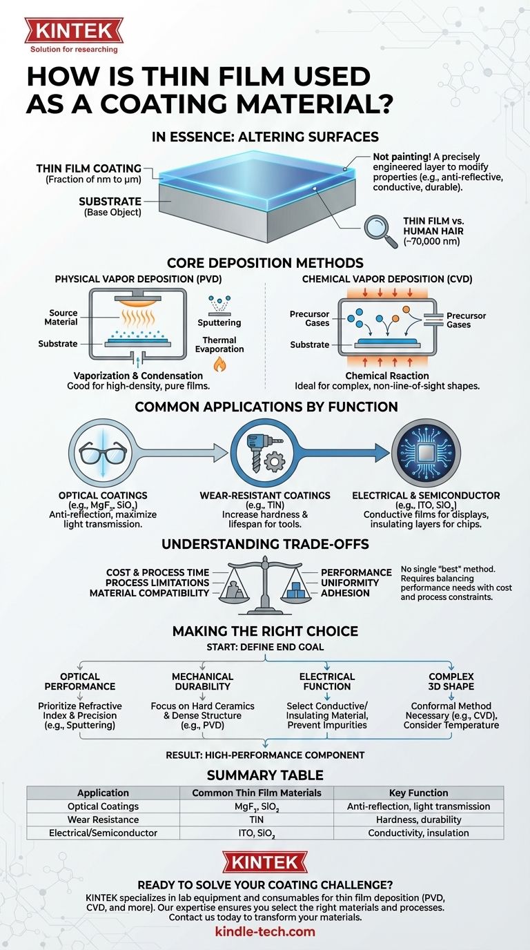
In essence, a thin film is used as a coating by depositing a microscopically thin, precisely engineered layer of material onto a surface, known as a substrate. This process is not like painting; it is a highly controlled technique designed to fundamentally alter the substrate's properties, such as making it anti-reflective, electrically conductive, or resistant to wear and corrosion. The specific material and deposition method are chosen to achieve a desired functional outcome.
The critical challenge in using thin films is not simply applying a layer, but strategically selecting the right combination of material, deposition process, and film structure to solve a specific engineering problem. The coating's success is defined by how well these choices align with the application's unique demands.
What is a Thin Film Coating?
Defining the Scale
A thin film is a layer of material ranging from fractions of a nanometer to several micrometers in thickness. To put this in perspective, a typical human hair is about 70,000 nanometers thick. This extreme thinness allows the film to add function without significantly changing the physical dimensions or weight of the object it coats.
The Goal: Modifying Surface Properties
The primary purpose of a thin film coating is to grant the surface of a substrate properties it does not naturally possess. This is a highly efficient way to create high-performance components, as the bulk of the object can be made from a cost-effective material while the critical surface functions are handled by the specialized thin film.
Substrate vs. Film
The relationship between the substrate (the base object) and the film (the coating) is crucial. The substrate provides the mechanical structure, while the film provides a specific function, such as optical filtering, electrical insulation, or hardness. Proper adhesion between the two is essential for the coating to be effective and durable.
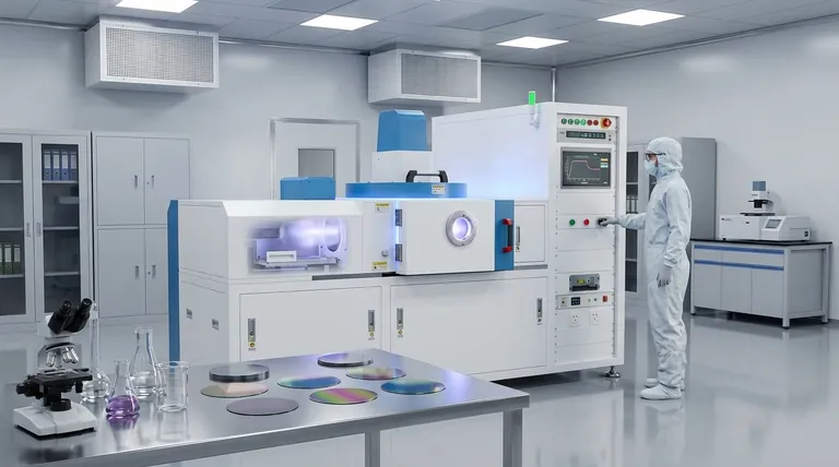
Core Deposition Methods: How Films are Made
The method used to create the film is as important as the material itself, as it dictates the film's density, uniformity, and adhesion. The two primary families of deposition are Physical Vapor Deposition and Chemical Vapor Deposition.
Physical Vapor Deposition (PVD)
In PVD processes, a solid or liquid source material is vaporized in a vacuum chamber. This vapor then travels and condenses onto the substrate, forming the thin film.
Common PVD techniques include sputtering, where ions bombard a target material to eject atoms, and thermal evaporation, where the source material is heated until it evaporates. PVD is excellent for creating very pure, high-density films.
Chemical Vapor Deposition (CVD)
CVD involves introducing precursor gases into a chamber containing the heated substrate. Chemical reactions occur on the substrate's surface, causing a solid film to grow.
This method is excellent for coating complex, non-line-of-sight geometries, as the gas can reach all exposed surfaces. It is fundamental to the manufacturing of semiconductors and other electronic components.
Common Applications by Function
The versatility of thin films is best understood through their real-world applications.
Optical Coatings
Materials like magnesium fluoride (MgF₂) and silicon dioxide (SiO₂) are used to create anti-reflection coatings on eyeglass lenses, camera lenses, and solar panels, maximizing light transmission.
Wear-Resistant Coatings
Hard materials such as titanium nitride (TiN) are deposited onto cutting tools, drills, and machine components. This dramatically increases their hardness and lifespan, allowing them to operate at higher speeds.
Electrical & Semiconductor Coatings
Transparent conductive films like indium tin oxide (ITO) are essential for touch screens and flat-panel displays. In microchip fabrication, layers of materials like silicon dioxide are used to create the insulating and conductive pathways that form transistors.
Understanding the Trade-offs
Choosing a thin film solution requires a clear understanding of the inherent compromises. There is no single "best" method or material; there is only the best fit for a specific application.
Cost vs. Performance
Highly specialized processes like Atomic Layer Deposition (ALD), a subtype of CVD that offers unparalleled thickness control, are significantly more expensive and slower than general-purpose methods like thermal evaporation. The required performance must justify the cost.
Process Limitations
PVD is often a "line-of-sight" process, making it difficult to uniformly coat complex 3D shapes. Conversely, CVD can handle complex shapes but often requires high temperatures that could damage heat-sensitive substrates like plastics.
Material Compatibility
Not all materials can be successfully deposited on all substrates. Issues like poor adhesion or a mismatch in thermal expansion coefficients can cause the film to peel, crack, or delaminate when subjected to temperature changes.
Making the Right Choice for Your Application
To select the appropriate thin film coating, you must begin with your end goal.
- If your primary focus is optical performance: Prioritize materials with the required refractive index and a deposition process, like sputtering, that guarantees precise thickness control.
- If your primary focus is mechanical durability: Focus on hard ceramic materials like nitrides or carbides and a PVD process that ensures a dense, strongly adhered film structure.
- If your primary focus is electrical function: The choice of material (e.g., a metal for conductivity or an oxide for insulation) is paramount, and the process must prevent impurities that would degrade performance.
- If your primary focus is coating a complex 3D shape: A conformal method like CVD will likely be necessary, and the substrate material must be able to withstand the required process temperatures.
By meticulously aligning the material, its form, and the deposition process with your specific goal, you can transform a standard material into a high-performance, functional component.
Summary Table:
| Application | Common Thin Film Materials | Key Function |
|---|---|---|
| Optical Coatings | Magnesium Fluoride (MgF₂), Silicon Dioxide (SiO₂) | Anti-reflection, light transmission |
| Wear Resistance | Titanium Nitride (TiN) | Hardness, durability for tools |
| Electrical/Semiconductor | Indium Tin Oxide (ITO), Silicon Dioxide (SiO₂) | Conductivity, insulation for displays/chips |
Ready to solve your coating challenge with precision thin films? KINTEK specializes in lab equipment and consumables for thin film deposition, offering solutions for PVD, CVD, and more. Whether you need to enhance optical performance, increase wear resistance, or achieve specific electrical properties, our expertise ensures you select the right materials and processes for your substrate. Contact us today to discuss how we can help you transform your materials into high-performance components.
Visual Guide
Related Products
- Aluminum-Plastic Flexible Packaging Film for Lithium Battery Packaging
- Thin-Layer Spectral Electrolysis Electrochemical Cell
People Also Ask
- What is the difference between monolayer and multilayer film? Choose the Right Packaging for Your Product
- What is organic thin film? A Guide to Engineered Molecular Layers for Advanced Tech
- What are the three types of lamination? Choose the Perfect Finish for Your Print Project
- What are the properties of Aluminium (Al) relevant to its use in coatings? High Reflectivity & Conductivity Explored
- What is the difference between single layer film and multi layer film? A Guide to Material Selection

