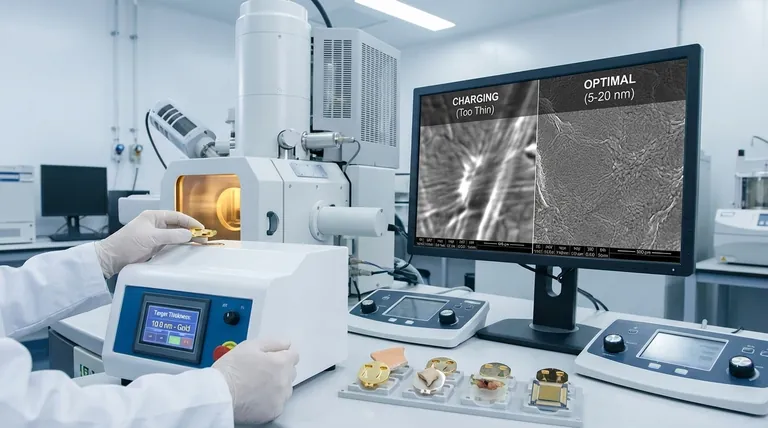
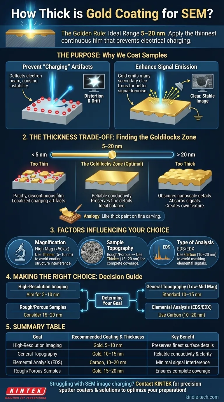
For most SEM applications, the ideal gold or gold-palladium coating thickness is between 5 and 20 nanometers (nm). This range is the standard because it's thick enough to make a non-conductive sample electrically conductive, preventing image distortion, yet thin enough that it doesn't obscure the sample's true surface morphology.
The goal is not to achieve a specific number, but to apply the thinnest possible continuous film that effectively prevents electrical charging. This preserves the finest surface details of your sample while ensuring a clear, stable image.
The Purpose of Gold Coating in SEM
Understanding why we coat samples is the key to determining the correct thickness. The metallic layer serves two primary functions that are critical for imaging non-conductive materials like polymers, ceramics, or biological specimens.
Preventing "Charging" Artifacts
A Scanning Electron Microscope (SEM) scans a sample with a high-energy beam of electrons. When these electrons strike a non-conductive surface, they accumulate, creating a localized negative charge.
This "charging" effect deflects the incoming electron beam and interferes with the signals leaving the sample, resulting in bright, distorted patches, streaks, and a loss of image stability. A thin, continuous gold coating provides a conductive path for this excess charge to be safely conducted away to the grounded sample holder.
Enhancing Signal Emission
The most common imaging mode in SEM relies on detecting secondary electrons (SE), which are low-energy electrons ejected from the sample's surface. Heavy metals like gold are exceptionally efficient at emitting secondary electrons.
By coating the sample, you create a surface that generates a strong, clear signal. This improves the signal-to-noise ratio, leading to sharper, higher-contrast images of the surface topography.
Understanding the Trade-offs of Coating Thickness
The thickness of your coating is a critical parameter that involves a direct trade-off between conductivity and image fidelity. Both too little and too much gold will compromise your results.
The Problem with "Too Thin" (< 5 nm)
A coating that is too thin may not form a continuous, unbroken film over the sample's surface. It can be patchy, like a series of tiny islands.
These discontinuities fail to provide a complete path for electrons to escape, leading to localized charging artifacts. If you see bright, unstable areas in your image, your coating is likely too thin or incomplete.
The Problem with "Too Thick" (> 20 nm)
A thick coating can obscure the very features you want to see. As the gold layer builds up, it begins to create its own surface texture, masking the sample's native nanoscale details.
Think of it like applying a thick layer of paint to a finely carved wooden object—you quickly lose all the subtle details. Furthermore, a thick coating can absorb signals from the sample itself, which is particularly problematic for other analytical techniques like elemental analysis.
The Goldilocks Zone (5-20 nm)
This range represents the optimal balance for most general-purpose imaging. It is robust enough to cover minor surface irregularities and reliably prevent charging, without significantly altering the surface texture at low to moderate magnifications.
Factors Influencing Your Choice of Thickness
The ideal thickness is not a single number but depends entirely on your sample and your analytical goals.
Desired Magnification
At very high magnifications (e.g., >50,000x), even the fine granular structure of a 10 nm gold film can become visible and interfere with your interpretation of the sample's true surface.
For high-resolution work, you must use the thinnest possible continuous coating (typically 5-10 nm) to minimize these artifacts. For low-magnification overviews, a thicker, more forgiving coating is acceptable.
Sample Topography
Samples with very complex, rough, or porous surfaces are more challenging to coat evenly. Deep crevices or sharp angles can be "shadowed" during the coating process.
For these samples, a slightly thicker coating (in the 15-20 nm range) may be necessary to ensure a continuous conductive layer across the entire complex surface.
Type of Analysis (Imaging vs. Composition)
If your goal is Energy-Dispersive X-ray Spectroscopy (EDS/EDX) for elemental analysis, the coating is a significant concern.
A thick gold coating can absorb the characteristic X-rays generated by lighter elements within your sample, preventing them from reaching the detector and leading to inaccurate results. For this reason, carbon coating is the standard for EDS, as carbon is a light element that interferes much less with the analysis. If gold must be used, it should be kept exceptionally thin (<5 nm).
Making the Right Choice for Your Goal
Before you head to the sputter coater, consider your primary objective.
- If your primary focus is high-resolution imaging: Aim for the thinnest possible continuous film, typically in the 5-10 nm range, to preserve the finest surface details.
- If your primary focus is general topographical analysis at low-to-mid magnification: A standard coating of 10-15 nm is a reliable and robust choice that guarantees good conductivity.
- If your primary focus is elemental analysis (EDS/EDX): Avoid gold if possible. The best practice is to use a 10-20 nm carbon coating, which provides conductivity without masking elemental signals.
- If you are imaging a very rough or porous sample: You may need a slightly thicker coating, perhaps 15-20 nm, to ensure complete coverage and prevent charging in deep features.
Ultimately, the optimal coating thickness is a strategic choice that directly impacts the quality and accuracy of your SEM results.
Summary Table:
| Goal | Recommended Coating & Thickness | Key Benefit |
|---|---|---|
| High-Resolution Imaging | Gold, 5-10 nm | Preserves finest surface details |
| General Topography (Low-Mid Mag) | Gold, 10-15 nm | Reliable conductivity & clarity |
| Elemental Analysis (EDS/EDX) | Carbon, 10-20 nm | Minimal interference with sample signals |
| Rough/Porous Samples | Gold, 15-20 nm | Ensures complete coverage of complex surfaces |
Struggling with SEM image charging or loss of detail? The right coating thickness is critical for clear, accurate results. At KINTEK, we specialize in lab equipment and consumables for all your sample preparation needs, including precision sputter coaters and coatings tailored for SEM analysis. Our experts can help you select the ideal solution to enhance your imaging and analytical outcomes. Contact us today to optimize your SEM sample preparation!
Visual Guide
Related Products
People Also Ask
- What is the recommended pre-treatment procedure for gold or platinum sheets before use? Ensure a Pristine, Reproducible Surface
- What post-treatment procedures should be followed after using a gold plate electrode? Ensure Long-Term Accuracy & Performance
- What are the disadvantages of gold electrodes? Key Limitations for Your Lab Projects
- What are gold electrodes used for? Achieve Unmatched Sensitivity in Biosensing and Research
- How should contamination of a gold plate electrode be prevented and managed? Essential Care for Reliable Data