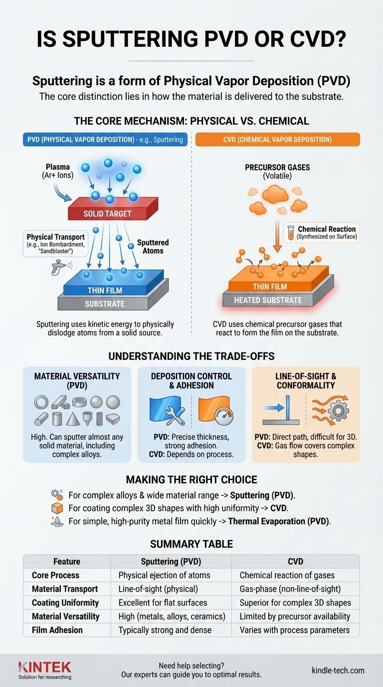
To be clear, sputtering is a form of Physical Vapor Deposition (PVD). It is fundamentally a physical process where high-energy ions bombard a solid source material, called a target, to physically dislodge atoms that then deposit onto a substrate. It is distinct from Chemical Vapor Deposition (CVD), which relies on chemical reactions to form a film.
The core distinction lies in how the material is delivered to the substrate. PVD, including sputtering, physically transports atoms from a solid source to the substrate. CVD uses chemical precursor gases that react on the substrate's surface to create the desired material.

The Core Mechanism: Physical vs. Chemical Deposition
To truly understand why sputtering is PVD, you must grasp the difference between a physical and a chemical deposition process. The name itself holds the key.
How Sputtering Works (A Physical Process)
Sputtering begins by creating a plasma, typically from an inert gas like argon, within a vacuum chamber. This plasma contains positively charged argon ions.
An electric field accelerates these ions, causing them to collide with the source material (the "target") with great force.
Think of it as a microscopic sandblaster. Each ion impact has enough energy to physically knock atoms loose from the target's surface. These ejected atoms travel through the chamber and condense on the substrate, building up a thin film layer by layer.
The Defining Characteristic of PVD
Physical Vapor Deposition is a family of processes defined by this mechanism: a solid material is converted into a vapor phase and then transported to condense on a substrate.
Sputtering achieves this vaporization through kinetic energy (ion bombardment). Another common PVD method, thermal evaporation, achieves it through thermal energy (heating the material until it evaporates). In both cases, the material itself is physically moved, not chemically created.
How CVD Differs (A Chemical Process)
Chemical Vapor Deposition is entirely different. In CVD, one or more volatile precursor gases are introduced into a reaction chamber.
These gases decompose or react with each other on the surface of a heated substrate, leaving behind a solid film. The film material is synthesized directly on the substrate through a chemical reaction, not transported from a source target.
Understanding the Trade-offs
Choosing between PVD and CVD involves understanding their inherent advantages and limitations, which stem directly from their physical or chemical nature.
Material Versatility
Sputtering (PVD) is exceptionally versatile. Almost any material that can be fabricated into a solid target—including pure metals, alloys, and even some ceramic compounds—can be sputtered.
CVD, in contrast, requires specific, often complex, and sometimes hazardous precursor chemicals that can reliably react to form the desired film.
Deposition Control and Adhesion
Sputtering provides excellent control over film thickness and uniformity. The high energy of the sputtered atoms also typically results in dense films with strong adhesion to the substrate.
Line-of-Sight Limitation
A key challenge for most PVD processes, including sputtering, is that they are "line-of-sight." The sputtered atoms travel in relatively straight lines from the target to the substrate. This can make it difficult to uniformly coat complex, three-dimensional shapes with undercuts or hidden surfaces.
Because CVD relies on gas transport, it can often provide more "conformal" coatings that cover complex geometries more uniformly.
Making the Right Choice for Your Goal
The decision to use sputtering or another method depends entirely on the application's requirements.
- If your primary focus is depositing a wide range of materials, including complex alloys: Sputtering (PVD) is an excellent and highly controllable choice due to its use of physical targets.
- If your primary focus is coating complex 3D shapes with high uniformity: Chemical Vapor Deposition (CVD) may be more suitable, as the chemical reaction can occur on all exposed surfaces.
- If your primary focus is depositing a simple, high-purity metal film quickly: Thermal Evaporation (another PVD method) can sometimes be a simpler and faster alternative to sputtering.
Understanding this fundamental distinction between physical and chemical processes empowers you to select the right thin-film technology for your specific application.
Summary Table:
| Feature | Sputtering (PVD) | CVD |
|---|---|---|
| Core Process | Physical ejection of atoms from a target | Chemical reaction of precursor gases on substrate |
| Material Transport | Line-of-sight | Gas-phase (non-line-of-sight) |
| Coating Uniformity | Excellent for flat surfaces | Superior for complex 3D shapes |
| Material Versatility | High (metals, alloys, ceramics) | Limited by precursor availability |
| Film Adhesion | Typically strong and dense | Varies with process parameters |
Need help selecting the right deposition technology for your application? KINTEK specializes in lab equipment and consumables, serving laboratory needs. Our experts can help you choose between PVD (like sputtering) and CVD systems to achieve optimal thin-film results for your specific materials and geometries. Contact us today to discuss your project requirements!
Visual Guide
Related Products
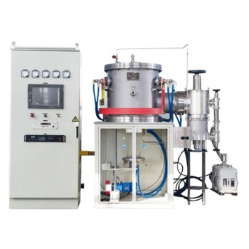
- RF PECVD System Radio Frequency Plasma-Enhanced Chemical Vapor Deposition RF PECVD
- Chemical Vapor Deposition CVD Equipment System Chamber Slide PECVD Tube Furnace with Liquid Gasifier PECVD Machine
- VHP Sterilization Equipment Hydrogen Peroxide H2O2 Space Sterilizer
- Split Chamber CVD Tube Furnace with Vacuum Station Chemical Vapor Deposition System Equipment Machine
- Electric Heated Hydraulic Vacuum Heat Press for Lab
People Also Ask
- What are the advantages of PECVD? Enable Low-Temperature, High-Quality Thin-Film Deposition
- Why is PECVD environment friendly? Understanding the Eco-Friendly Benefits of Plasma-Enhanced Coating
- What are the applications of PECVD? Essential for Semiconductors, MEMS, and Solar Cells
- Why does PECVD commonly use RF power input? For Precise Low-Temperature Thin Film Deposition
- How does RF power create plasma? Achieve Stable, High-Density Plasma for Your Applications