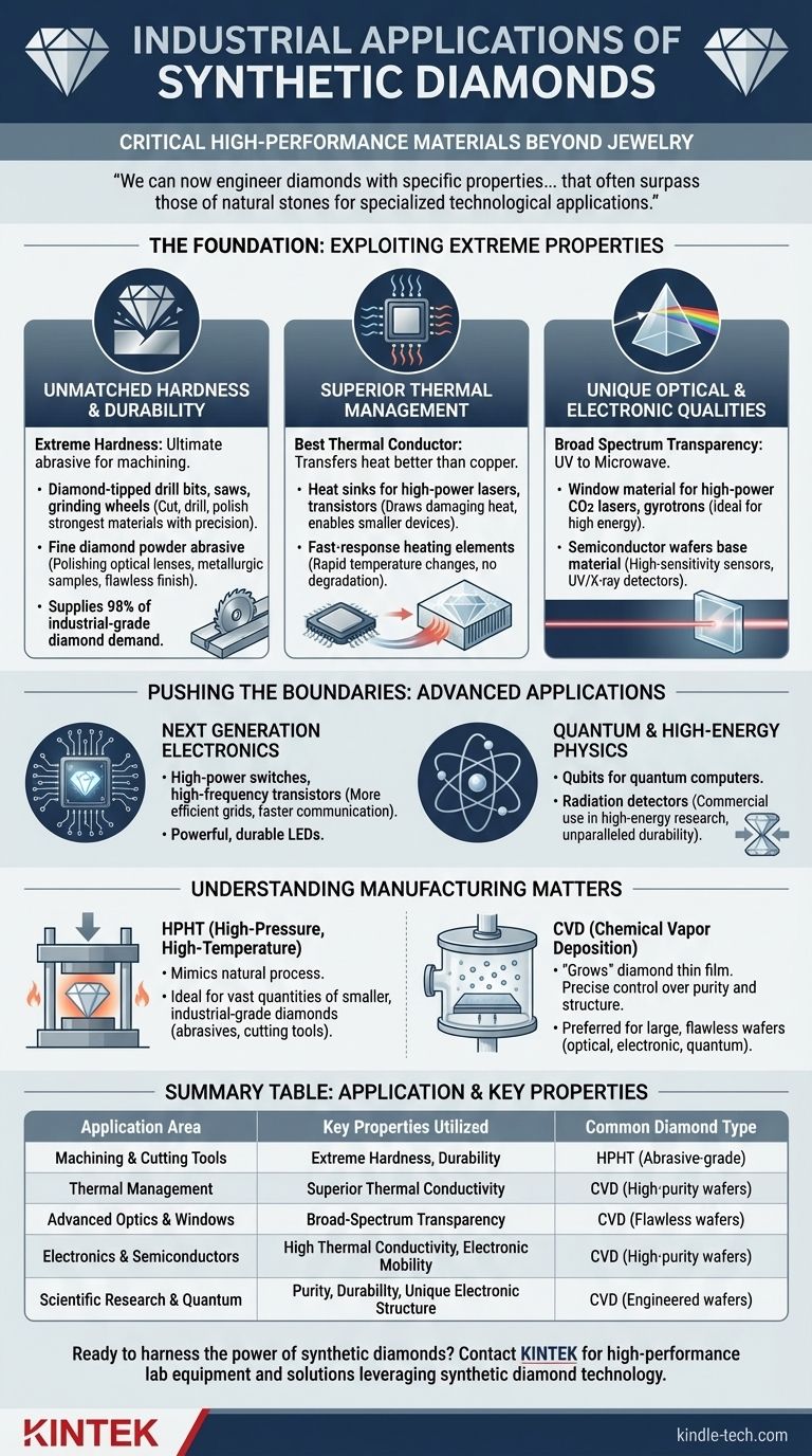
In modern industry, synthetic diamonds are a critical high-performance material, far removed from their jewelry counterparts. Their primary uses are centered on tasks that demand extreme physical properties, including machining and cutting tools, managing heat in advanced electronics, and serving as transparent armor or windows for high-power lasers and sensors.
The core reason for the industrial dominance of synthetic diamonds is not simply cost, but control. We can now engineer diamonds with specific properties—like superior hardness, thermal conductivity, and electronic mobility—that often surpass those of natural stones for specialized technological applications.
The Foundation: Exploiting Diamond's Extreme Properties
The wide range of industrial uses for synthetic diamonds stems directly from their unique and powerful combination of physical characteristics. Unlike other materials, diamond excels in multiple domains simultaneously.
Unmatched Hardness and Durability
The most well-known property of diamond is its extreme hardness. This makes it the ultimate material for abrasive and machining operations.
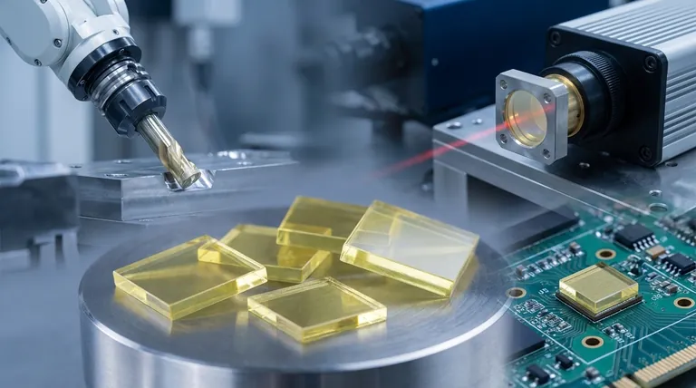
Synthetic diamonds are used to create diamond-tipped drill bits, saws, and grinding wheels. They can cut, drill, and polish the world's strongest materials with high precision.
Fine diamond powder is also a leading abrasive, used for polishing everything from optical lenses to metallurgic samples where a flawless finish is required. It's estimated that synthetic diamonds supply 98% of all industrial-grade diamond demand for these applications.
Superior Thermal Management
Diamond is one of the best thermal conductors known to science, transferring heat more effectively than copper. This property is critical for high-power electronics where heat is the primary limiting factor.
They are used as heat sinks for high-power lasers and transistors, rapidly drawing damaging heat away from sensitive components. This allows for smaller, more powerful electronic devices.
This thermal stability is also key to their use in fast-response heating elements and other applications requiring rapid temperature changes without material degradation.
Unique Optical and Electronic Qualities
High-purity synthetic diamond is transparent across an exceptionally broad spectrum of light, from ultraviolet to far-infrared and even microwaves.
This makes it an ideal window material for high-power CO2 lasers and gyrotrons, where other materials would crack or absorb too much energy.
Its unique electronic structure also allows it to be used as a base material for semiconductor wafers, high-sensitivity temperature sensors, and detectors for UV, X-ray, and other forms of radiation.
Pushing the Boundaries: Advanced and Future Applications
The ability to create large, ultra-pure diamond wafers through methods like Chemical Vapor Deposition (CVD) is unlocking applications that were once theoretical.
The Next Generation of Electronics
Synthetic diamonds are being developed for high-power switches and high-frequency field-effect transistors. Their properties could lead to more efficient power grids and faster communication systems.
They are also being explored for creating powerful and durable light-emitting diodes (LEDs).
Quantum and High-Energy Physics
Specially engineered synthetic diamonds serve as the base material for qubits, the fundamental building blocks of quantum computers.
Diamond-based radiation detectors are already in commercial use at high-energy research facilities, offering unparalleled durability and performance in harsh environments.
Specialized Scientific Instruments
Diamond anvils, made from two opposing synthetic diamonds, are used to study how materials behave under immense pressures—up to 2.5 million times normal atmospheric pressure.
They are also used to create ultra-sharp needles for scanning probe microscopes, enabling researchers to view and manipulate matter at the atomic level.
Understanding the Trade-offs: Manufacturing Matters
The properties of a synthetic diamond, and thus its application, are determined by how it was made. Not all synthetic diamonds are created equal.
High-Pressure, High-Temperature (HPHT)
The HPHT method mimics the natural diamond-forming process by subjecting carbon to immense pressure and heat.
This process is highly effective for creating vast quantities of smaller, industrial-grade diamonds, making it ideal for abrasives and cutting tools.
Chemical Vapor Deposition (CVD)
The CVD method "grows" diamond as a thin film in a vacuum chamber, building it up layer by layer.
This technique allows for precise control over the diamond's purity and structure. It is the preferred method for creating large, flawless wafers needed for optical, electronic, and quantum applications.
How to Apply This to Your Goal
The right type of synthetic diamond is entirely dependent on the problem you are trying to solve.
- If your primary focus is mechanical applications (cutting, grinding): Robust and cost-effective abrasive-grade diamonds, typically made via HPHT, are the industry standard.
- If your primary focus is thermal management or electronics: High-purity, thermally conductive diamond wafers, almost always made via CVD, are essential for dissipating heat effectively.
- If your primary focus is advanced optics or research: Flawless, custom-engineered CVD diamonds are necessary to meet the extreme purity and transparency requirements for lasers, sensors, and quantum devices.
Ultimately, engineered diamonds have become a foundational material, enabling progress in virtually every area of high technology.
Summary Table:
| Application Area | Key Properties Utilized | Common Diamond Type |
|---|---|---|
| Machining & Cutting Tools | Extreme Hardness, Durability | HPHT (Abrasive-grade) |
| Thermal Management | Superior Thermal Conductivity | CVD (High-purity wafers) |
| Advanced Optics & Windows | Broad-Spectrum Transparency | CVD (Flawless wafers) |
| Electronics & Semiconductors | High Thermal Conductivity, Electronic Mobility | CVD (High-purity wafers) |
| Scientific Research & Quantum | Purity, Durability, Unique Electronic Structure | CVD (Engineered wafers) |
Ready to harness the power of synthetic diamonds in your lab or production line? KINTEK specializes in providing high-performance lab equipment and consumables, including solutions that leverage synthetic diamond technology. Whether you need robust cutting tools or advanced thermal management components, our expertise can help you achieve superior results. Contact our experts today to discuss how we can support your specific industrial or research needs!
Visual Guide
Related Products
- CVD Diamond for Thermal Management Applications
- CVD Diamond Optical Windows for Lab Applications
- Custom CVD Diamond Coating for Lab Applications
- Laboratory CVD Boron Doped Diamond Materials
- CVD Diamond Domes for Industrial and Scientific Applications
People Also Ask
- What is the hardness of CVD diamond? The Ultimate Guide to Engineered Super-Materials
- How long does it take to make a CVD diamond? A Detailed Look at the Growth Timeline
- Will a CVD diamond pass a diamond tester? Yes, because it's a real diamond.
- Are CVD diamonds real or fake? Discover the Truth About Lab-Grown Diamonds
- How long does it take to grow a CVD diamond? A 2-4 Week Journey to a Flawless Gem


