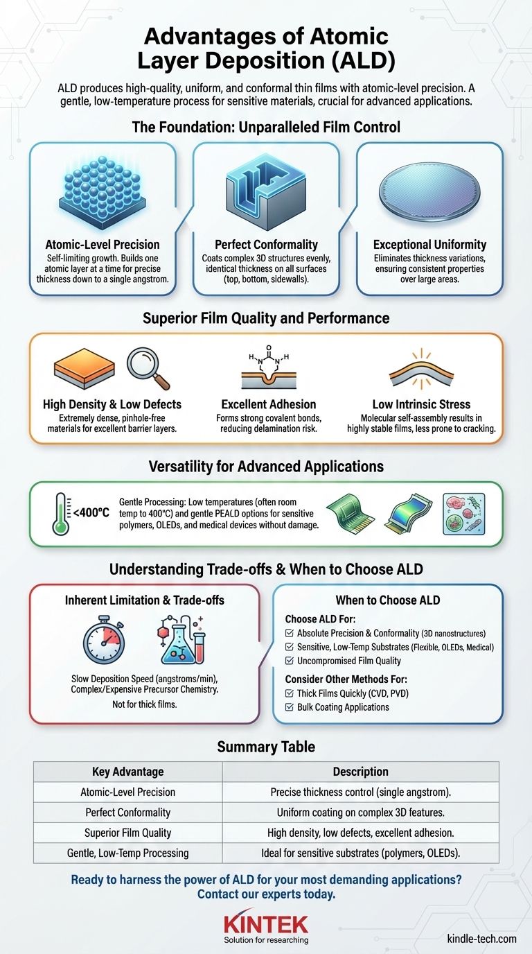
The primary advantages of Atomic Layer Deposition (ALD) are its ability to produce exceptionally high-quality, uniform, and conformal thin films with atomic-level precision. Because it is a gentle, low-temperature process, it can be used on a wide range of sensitive materials that other deposition techniques would damage, such as polymers and OLEDs. This combination of precision and versatility makes it a critical technology for advanced applications.
The power of ALD is rooted in its fundamental mechanism: a self-limiting, layer-by-layer growth process. This inherent atomic control is the direct source of its signature advantages, from perfect conformity on complex shapes to superior film quality on delicate materials.
The Foundation: Unparalleled Film Control
The defining characteristic of ALD is its sequential, self-limiting nature. This process separates it from other thin-film techniques and is the source of its most significant benefits.
Atomic-Level Thickness Precision
ALD builds films one atomic layer at a time. Each deposition cycle consists of sequential pulses of chemical precursors, and each pulse reaction stops once all available surface sites are occupied.
This self-limiting behavior means the film growth per cycle is a constant. This allows for the deposition of films with precisely controlled thickness, down to a single angstrom.
Perfect Conformality
Because the precursors are introduced as a gas in sequential steps, they can penetrate and coat even the most complex, high-aspect-ratio 3D structures. The chemical reaction occurs uniformly on every exposed surface.
This results in a film that is perfectly conformal, meaning its thickness is identical on the top, bottom, and sidewalls of any feature, which is extremely difficult to achieve with line-of-sight methods like PVD (Physical Vapor Deposition).
Exceptional Uniformity
The self-limiting reactions ensure that the film grows uniformly across the entire substrate. This eliminates the thickness variations common in other techniques, ensuring consistent material properties over large areas, such as an entire silicon wafer.
Superior Film Quality and Performance
The controlled, layer-by-layer growth mechanism translates directly into higher-quality materials with enhanced performance characteristics.
High Density and Low Defects
ALD films are grown in a highly controlled manner, resulting in materials that are extremely dense and virtually free of pinholes or other defects. This is critical for applications like creating hermetic barrier layers that protect against moisture and oxygen.
Excellent Adhesion
The first cycle of an ALD process forms strong covalent bonds directly with the substrate surface. This chemical anchoring provides superior adhesion compared to physically deposited films, reducing the risk of delamination.
Low Intrinsic Stress
Films are built up slowly and methodically through what is effectively molecular self-assembly. This low-energy process results in films with very low intrinsic stress, making them highly stable and less prone to cracking, especially when depositing on flexible substrates.
Versatility for Advanced Applications
ALD’s unique process window opens the door to coating materials and structures that are inaccessible to conventional methods.
Gentle Processing for Sensitive Substrates
ALD can be performed at low temperatures, often from room temperature up to 400°C. When combined with low-power plasma (PEALD), the process is gentle enough to deposit high-quality films on sensitive materials like polymers, flexible electronics, OLEDs, and even biological samples without causing thermal damage.
Understanding the Trade-offs
While powerful, ALD is not the universal solution for all thin-film needs. Its primary limitation is a direct consequence of its greatest strength.
The Inherent Limitation: Deposition Speed
Because ALD builds films one atomic layer at a time, it is an inherently slow process. Deposition rates are typically measured in angstroms per minute.
For applications requiring thick films (microns or more), other methods like Chemical Vapor Deposition (CVD) or sputtering are often far more practical and cost-effective.
Precursor Chemistry and Cost
ALD relies on highly reactive chemical precursors. Developing and sourcing the correct precursor pairs for a specific material can be complex and expensive, and a robust process may not be available for every element or compound.
When to Choose ALD
Selecting the right deposition technique requires aligning the method's strengths with your primary goal.
- If your primary focus is absolute precision and conformality: ALD is the definitive choice for coating complex 3D nanostructures or depositing ultrathin gate dielectrics.
- If you are working with sensitive, low-temperature substrates: ALD's gentle, low-temperature capability is a key enabler for advanced applications in flexible electronics, OLEDs, and medical devices.
- If your primary focus is creating thick films quickly: Other methods like CVD or PVD are almost always more cost-effective and suitable for bulk coating applications.
Ultimately, ALD is the premier solution when the quality, precision, and performance of the film cannot be compromised.
Summary Table:
| Key Advantage | Description |
|---|---|
| Atomic-Level Precision | Precise film thickness control, down to a single angstrom. |
| Perfect Conformality | Uniform coating on complex 3D structures, including high-aspect-ratio features. |
| Superior Film Quality | High density, low defects, excellent adhesion, and low intrinsic stress. |
| Gentle, Low-Temp Processing | Ideal for sensitive substrates like polymers, OLEDs, and flexible electronics. |
Ready to harness the power of ALD for your most demanding applications?
At KINTEK, we specialize in providing advanced lab equipment and consumables tailored to your research and production needs. Whether you're developing next-generation electronics, medical devices, or nanomaterials, our expertise in thin-film deposition solutions can help you achieve unparalleled precision and performance.
Contact our experts today to discuss how ALD technology can solve your specific challenges and elevate your laboratory's capabilities.
Visual Guide
Related Products
- Aluminized Ceramic Evaporation Boat for Thin Film Deposition
- RF PECVD System Radio Frequency Plasma-Enhanced Chemical Vapor Deposition RF PECVD
- Ceramic Evaporation Boat Set Alumina Crucible for Laboratory Use
- Custom CVD Diamond Coating for Lab Applications
People Also Ask
- Why is an alumina boat selected for catalyst precursors? Ensure Sample Purity at 1000 °C
- Why is an alumina boat and Ti3AlC2 powder bed necessary for Ti2AlC sintering? Protect MAX Phase Purity
- Why are high-purity ceramic boats used for lignin activation? Ensure Purity & Thermal Stability
- What are the alternatives to sputtering? Choose the Right Thin Film Deposition Method
- What is the source of evaporation for thin film? Choosing Between Thermal and E-Beam Methods


