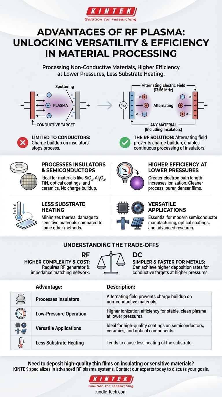
The primary advantages of RF plasma are its ability to process non-conductive (insulating) materials, its higher operational efficiency at lower gas pressures, and its tendency to cause less heating of the substrate. Unlike Direct Current (DC) systems, which are limited to conductive targets, Radio Frequency (RF) plasma's alternating electric field makes it a far more versatile tool for a wide range of modern applications, from semiconductor manufacturing to optical coatings.
The core limitation of DC plasma is its reliance on a continuous electrical circuit. RF plasma overcomes this by using a rapidly alternating electric field, which prevents charge buildup on insulating surfaces and creates a more efficient, stable plasma at lower pressures.
Why RF Plasma Excels Where DC Falters
To appreciate the advantages of RF plasma, it's essential to understand the fundamental problem it solves. DC systems are simpler, but their physics impose a critical limitation that RF was designed to overcome.
The Charge Buildup Problem on Insulators
In a standard DC sputtering system, a target material is bombarded by positive ions from the plasma. This process requires the target to be electrically conductive to complete the circuit and replenish the electrons that are ejected.
If you use an insulating target, positive ions strike its surface and get stuck. This creates a positive charge layer that quickly begins to repel the incoming positive ions from the plasma, effectively shutting down the sputtering process.
The Alternating Field Solution
RF plasma solves this by applying an alternating voltage, typically at a frequency of 13.56 MHz.
During one half of the AC cycle, the target is negatively charged and attracts positive ions for sputtering. Crucially, during the other half-cycle, the target becomes positively charged, attracting electrons from the plasma. These electrons neutralize the positive charge that built up, "resetting" the surface for the next sputtering cycle. This rapid switching allows for the continuous processing of any material, regardless of its conductivity.
Higher Efficiency at Lower Pressures
The RF field causes free electrons within the plasma to oscillate at high speed. This greatly increases their path length and the probability that they will collide with and ionize neutral gas atoms.
This effect makes RF systems much more efficient at sustaining a dense plasma. As a result, they can operate effectively at much lower chamber pressures than DC systems. This low-pressure operation leads to a "cleaner" process with fewer gas particle collisions, resulting in higher-quality deposited films with better density and purity.
Understanding the Trade-offs
While powerful, RF plasma systems are not universally superior to DC systems. The choice involves clear trade-offs in complexity, cost, and application suitability.
System Complexity and Cost
An RF plasma system is inherently more complex than a DC one. It requires a specialized RF power generator and, critically, an impedance matching network (often called a "matchbox").
This network is necessary to efficiently transfer power from the generator to the plasma, whose electrical properties can change during operation. This added complexity increases the initial equipment cost and potential maintenance requirements.
Deposition Rates
The claim that RF is "10 times faster" must be contextualized. This is often true when comparing both systems at the same low pressure.
However, DC sputtering is typically run at higher pressures where it can achieve very high deposition rates for metals. For applications focused purely on depositing a thick metal film as quickly as possible, a DC system may still be the more economical and faster choice.
Process Control
The impedance matching required for an RF system adds a layer of process control complexity. The system must constantly adjust to ensure maximum power is delivered to the plasma and not reflected back to the generator. While modern systems automate this well, it is a variable that does not exist in simpler DC setups.
Making the Right Choice for Your Goal
Selecting the correct plasma source depends entirely on your material and desired outcome.
- If your primary focus is processing insulators or semiconductors: RF plasma is your only effective choice. This includes materials like silicon dioxide (SiO₂), aluminum oxide (Al₂O₃), or titanium nitride (TiN).
- If your primary focus is high-rate deposition of conductive metals: A DC system is often more cost-effective and can achieve higher throughput, assuming substrate heating and film purity at higher pressures are acceptable.
- If your primary focus is achieving the highest quality film: RF is generally superior. Its ability to operate at low pressures reduces gas incorporation in the film and allows for better control over the energy of depositing particles, leading to denser, purer coatings.
By understanding the fundamental physics of RF and DC plasma, you can confidently select the right tool to achieve your specific material processing goals.
Summary Table:
| Advantage | Description |
|---|---|
| Processes Insulators | Overcomes DC limitations by using an alternating field to prevent charge buildup on non-conductive materials. |
| Low-Pressure Operation | Higher ionization efficiency enables stable plasma at lower pressures for cleaner, higher-purity films. |
| Versatile Applications | Ideal for depositing high-quality coatings on semiconductors, ceramics, and optical components. |
| Less Substrate Heating | Tends to cause less heating of the substrate compared to some other plasma methods. |
Need to deposit high-quality thin films on insulating or sensitive materials?
KINTEK specializes in advanced lab equipment, including RF plasma systems for semiconductor manufacturing, optical coatings, and materials research. Our solutions are designed to deliver the precision, purity, and process control your application demands.
Contact our experts today to discuss how an RF plasma system can advance your research or production goals.
Visual Guide
Related Products
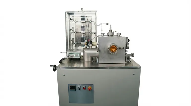
- RF PECVD System Radio Frequency Plasma-Enhanced Chemical Vapor Deposition RF PECVD
- Spark Plasma Sintering Furnace SPS Furnace
- Horizontal High Temperature Graphite Vacuum Graphitization Furnace
- XRF Boric Acid Lab Powder Pellet Pressing Mold for Laboratory Use
- Inclined Rotary Plasma Enhanced Chemical Vapor Deposition PECVD Equipment Tube Furnace Machine
People Also Ask
- What is plasma CVD? Unlock Low-Temperature Thin Film Deposition for Sensitive Materials
- What is plasma chemical vapor deposition? A Low-Temperature Thin Film Coating Solution
- What is plasma enhanced chemical vapour deposition process? Unlock Low-Temperature, High-Quality Thin Films
- What is the role of RF-PECVD in VFG preparation? Mastering Vertical Growth and Surface Functionality
- How does Radio Frequency Enhanced Plasma Chemical Vapour Deposition (RF-PECVD) work? Learn the Core Principles


