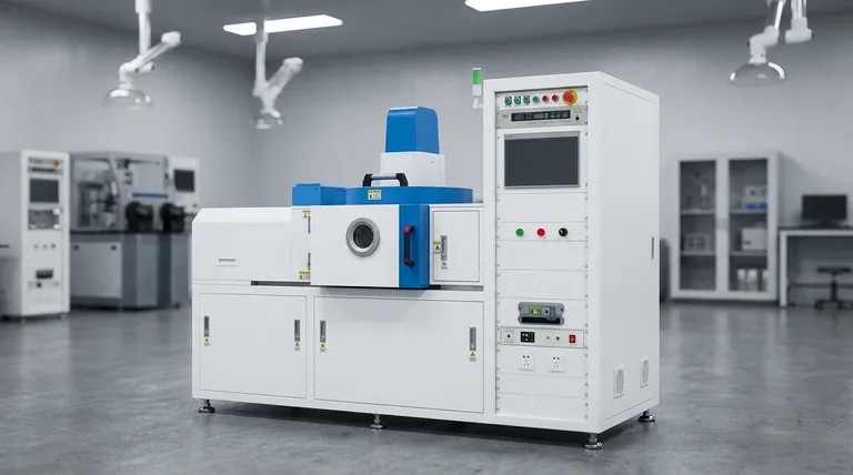
At its core, sputtering-based thin film deposition offers a unique combination of superior film quality and exceptional material versatility. This physical vapor deposition (PVD) technique uses high-energy plasma to bombard a target material, ejecting atoms that coat a substrate with a thin, highly uniform, and durable film. It excels where other methods fall short, particularly in applications demanding precise control and robust performance.
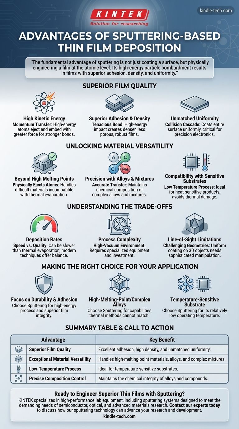
The fundamental advantage of sputtering is not just coating a surface, but physically engineering a film at the atomic level. Its high-energy particle bombardment results in films with superior adhesion, density, and uniformity, making it the definitive choice for high-performance applications across a vast range of materials.
Why Sputtering Excels in Film Quality
The quality of a thin film is defined by its adhesion, density, and uniformity. Sputtering's unique mechanism provides distinct advantages in all three areas.
The Role of High Kinetic Energy
Sputtering is fundamentally a process of momentum transfer. A noble gas plasma is accelerated to bombard a target, and the resulting collision ejects target atoms with significantly higher kinetic energy than those produced in thermal evaporation.
These high-energy atoms travel to the substrate and embed themselves with greater force, creating a stronger bond.
Superior Adhesion and Density
This high energy directly translates to better adhesion. The sputtered particles don't just land on the substrate; they impact it, creating a more tenacious and durable bond between the film and the underlying material.
This impact also results in films with higher packing densities, making them less porous and more robust.
Unmatched Uniformity
The process creates a collision cascade that coats the entire substrate surface. This allows for the creation of highly uniform films, a critical requirement in industries like semiconductors and optical devices where even minute variations can impact performance.
Unlocking Material Versatility
Beyond film quality, sputtering's primary advantage is its ability to work with an exceptionally broad palette of materials, many of which are incompatible with other deposition methods.
Beyond High Melting Points
Materials with very high melting points are extremely difficult or impossible to deposit using thermal evaporation. Because sputtering physically ejects atoms rather than melting and boiling them, it can easily handle these challenging materials.
Precision with Alloys and Mixtures
Sputtering maintains the chemical composition of complex materials like alloys and mixtures. It accurately transfers the material from the target to the substrate, enabling the creation of films with specific, engineered properties.
Compatibility with Sensitive Substrates
Compared to processes like Chemical Vapor Deposition (CVD), sputtering operates at relatively low temperatures. This makes it an ideal "dry process" for coating temperature-sensitive products or substrates that would be damaged by high-heat methods.
Understanding the Trade-offs
No single technology is a universal solution. To make an informed decision, it's critical to understand the context and limitations of sputtering.
Deposition Rates
While modern techniques like magnetron sputtering offer high deposition rates and precise control, some basic sputtering processes can be slower than methods like thermal evaporation. The choice of technique often involves a trade-off between speed and ultimate film quality.
Process Complexity
Sputtering requires a high-vacuum environment and specialized equipment to generate the gas plasma. This can make the initial investment in equipment more significant and the process more complex to manage than simpler deposition techniques.
Line-of-Sight Limitations
Like many PVD processes, sputtering is largely a "line-of-sight" technique. This means it can be challenging to achieve a perfectly uniform coating on complex, three-dimensional geometries without sophisticated substrate manipulation.
Making the Right Choice for Your Application
Selecting the correct deposition method depends entirely on your project's specific goals for performance, material compatibility, and substrate limitations.
- If your primary focus is maximum film durability and adhesion: Sputtering's high-energy process ensures a dense, strongly bonded film that is superior for demanding applications.
- If you need to deposit high-melting-point materials or complex alloys: Sputtering provides capabilities that thermal methods simply cannot match.
- If your substrate is temperature-sensitive: Sputtering's relatively low operating temperature offers a significant advantage over high-temperature processes like CVD.
Ultimately, sputtering provides an essential level of atomic-level control and quality required to create the high-performance components that define modern technology.
Summary Table:
| Advantage | Key Benefit |
|---|---|
| Superior Film Quality | Excellent adhesion, high density, and unmatched uniformity. |
| Exceptional Material Versatility | Handles high-melting-point materials, alloys, and complex mixtures. |
| Low-Temperature Process | Ideal for temperature-sensitive substrates. |
| Precise Composition Control | Maintains the chemical integrity of alloys and compounds. |
Ready to Engineer Superior Thin Films with Sputtering?
KINTEK specializes in high-performance lab equipment, including sputtering systems designed to meet the demanding needs of semiconductor, optical, and advanced materials research. Our solutions deliver the precise control, material versatility, and exceptional film quality your projects require.
Contact our experts today to discuss how our sputtering technology can advance your research and development.
Visual Guide
Related Products
- Spark Plasma Sintering Furnace SPS Furnace
- Vacuum Induction Melting Spinning System Arc Melting Furnace
- Chemical Vapor Deposition CVD Equipment System Chamber Slide PECVD Tube Furnace with Liquid Gasifier PECVD Machine
- Customer Made Versatile CVD Tube Furnace Chemical Vapor Deposition Chamber System Equipment
People Also Ask
- What is the theory of spark plasma sintering? A Guide to Rapid, Low-Temperature Densification
- What is SPS sintering method? A Guide to High-Speed, High-Performance Material Fabrication
- What is the mechanism of SPS process? A Deep Dive into Rapid, Low-Temperature Sintering
- What is the process fundamentals of spark plasma sintering? Achieve Rapid, High-Density Material Consolidation
- What are the advantages of CAMI/SPS for W-Cu composite preparation? Reduce cycles from hours to seconds.


