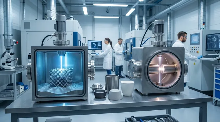
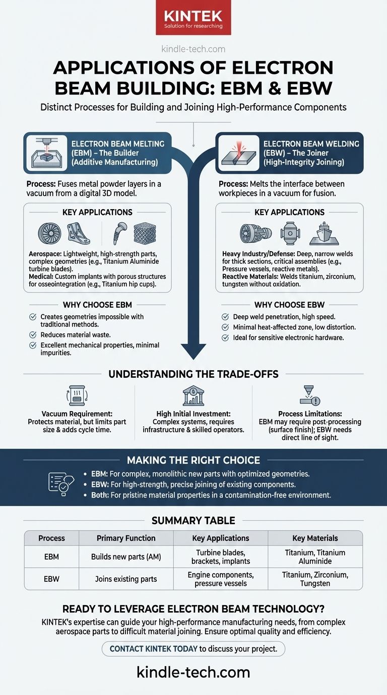
At its core, the term "electron beam building" refers to two distinct but related manufacturing processes. The first is Electron Beam Melting (EBM), a 3D printing method that builds parts from metal powder, and the second is Electron Beam Welding (EBW), which joins components together. Applications are concentrated in high-performance sectors like aerospace, medical, and defense, where the technology is used to create everything from jet engine turbine blades and medical implants to specialized electronic components and structural assemblies.
The central takeaway is that an electron beam is an energy source, not a single process. You must first distinguish whether your goal is to build a new part from scratch (EBM) or join existing parts together (EBW), as this determines the entire application and outcome.
The "Building" Process: Electron Beam Melting (EBM)
Electron Beam Melting is a form of powder bed fusion, an additive manufacturing (3D printing) technology. It uses a high-energy electron beam to melt and fuse layers of metal powder in a vacuum, constructing a fully dense, solid part from a digital 3D model.
Key Applications in Aerospace
EBM is heavily used to produce lightweight, high-strength components for aircraft and spacecraft. This includes complex parts like turbine blades, which benefit from the high-temperature capabilities of materials like titanium aluminide, and structural brackets with optimized, topology-driven designs that are impossible to machine traditionally.
Medical Implants and Devices
The technology is ideal for creating custom medical implants. Because EBM can process biocompatible materials like titanium and create intricate, porous lattice structures, it is used to manufacture orthopedic implants such as hip cups and spinal cages. The porous surface promotes osseointegration, where the patient's bone grows into the implant for a stronger, more permanent bond.
Why EBM is Chosen for These Tasks
EBM enables the creation of geometries that cannot be made with casting or machining, reduces material waste significantly, and produces parts with excellent mechanical properties. The high-temperature, vacuum environment minimizes impurities and residual stresses, resulting in parts that are often superior to those made by casting.
The "Joining" Process: Electron Beam Welding (EBW)
While EBM builds parts, EBW joins them. This process uses a finely focused electron beam to melt the interface between two workpieces, which then fuse together as the molten material cools. This is a high-energy-density joining process, not a building one.
Applications in Heavy Industry and Defense
EBW creates exceptionally deep and narrow welds, making it suitable for joining thick sections of metal. It is used for fabricating critical assemblies like aircraft engine components, pressure vessels, and potentially large structures such as ship shell plates or storage tanks where weld integrity is paramount.
Handling Difficult and Reactive Materials
The entire EBW process occurs in a vacuum, which prevents atmospheric contamination from oxygen or nitrogen. This makes it the preferred method for welding reactive metals like titanium and zirconium, as well as high-melting-point (refractory) metals like tungsten and molybdenum, which would otherwise oxidize or become brittle.
Why EBW is Chosen for These Tasks
EBW is valued for its deep weld penetration, high welding speed, and minimal heat-affected zone. This low heat input reduces part distortion, which is critical when joining precision-machined components for aerospace or sensitive electronic hardware.
Understanding the Trade-offs
Both EBM and EBW are powerful but specialized processes with shared limitations that are important to understand.
The Vacuum Requirement
The need for a high-vacuum chamber is the technology's greatest strength and biggest constraint. It protects the material but limits the maximum size of the part that can be built or welded and adds significant time to each cycle for pumping the chamber down.
High Initial Investment
Electron beam systems are complex and expensive to purchase, install, and maintain. They require significant infrastructure, including high-voltage power supplies and radiation shielding (due to X-ray generation), and demand highly skilled operators.
Process-Specific Limitations
EBM parts often have a rougher surface finish than those made with other additive methods and may require post-processing steps like machining. For EBW, the beam requires a direct line of sight to the joint, which can make it impossible to weld certain complex or hidden geometries.
Making the Right Choice for Your Application
Choosing the right electron beam process depends entirely on your manufacturing objective.
- If your primary focus is creating a complex, monolithic part from a digital design: EBM is the correct technology for additively manufacturing new components with optimized geometries and internal features.
- If your primary focus is joining two or more metal components with a high-strength, precise seam: EBW is the superior choice for high-integrity welding, especially for thick sections or reactive materials.
- If your primary focus is achieving pristine material properties with no atmospheric contamination: Both processes are ideal, as the shared vacuum environment protects the metal from oxidation and impurities.
Understanding this fundamental distinction between building and joining is the first step toward leveraging the power of electron beam technology for your specific engineering challenge.
Summary Table:
| Process | Primary Function | Key Applications | Key Materials |
|---|---|---|---|
| Electron Beam Melting (EBM) | Builds new parts (Additive Manufacturing) | Turbine blades, structural brackets, medical implants | Titanium, Titanium Aluminide |
| Electron Beam Welding (EBW) | Joins existing parts (High-integrity welding) | Aircraft engine components, pressure vessels, reactive metal assemblies | Titanium, Zirconium, Tungsten, Molybdenum |
Ready to leverage electron beam technology for your high-performance manufacturing needs?
Whether you are developing complex aerospace components, creating custom medical implants, or joining difficult materials, KINTEK's expertise in advanced lab and manufacturing equipment can help you achieve superior results. Our team can guide you in selecting the right technology for your specific application, ensuring optimal part quality and process efficiency.
Contact KINTEL today to discuss how our solutions can advance your projects in additive manufacturing and high-precision welding.
Visual Guide
Related Products
- E Beam Crucibles Electron Gun Beam Crucible for Evaporation
- Three-dimensional electromagnetic sieving instrument
- Electrolytic Electrochemical Cell for Coating Evaluation
- Customizable PEM Electrolysis Cells for Diverse Research Applications
- Custom PTFE Teflon Parts Manufacturer for Culture Dish and Evaporation Dish
People Also Ask
- What is the container that holds the metal source material called in e-beam evaporation? Ensure Purity and Quality in Your Thin-Film Deposition
- What is sputtering technology? A Guide to Precision Thin Film Deposition
- What is direct current DC magnetron sputtering? A Guide to High-Quality Thin Film Deposition
- What is sputter coating used for? Achieve Superior Thin Films for Electronics, Optics, and Tools
- What are the effects of magnetron sputtering? Achieve High-Quality, Durable Thin Films for Your Lab