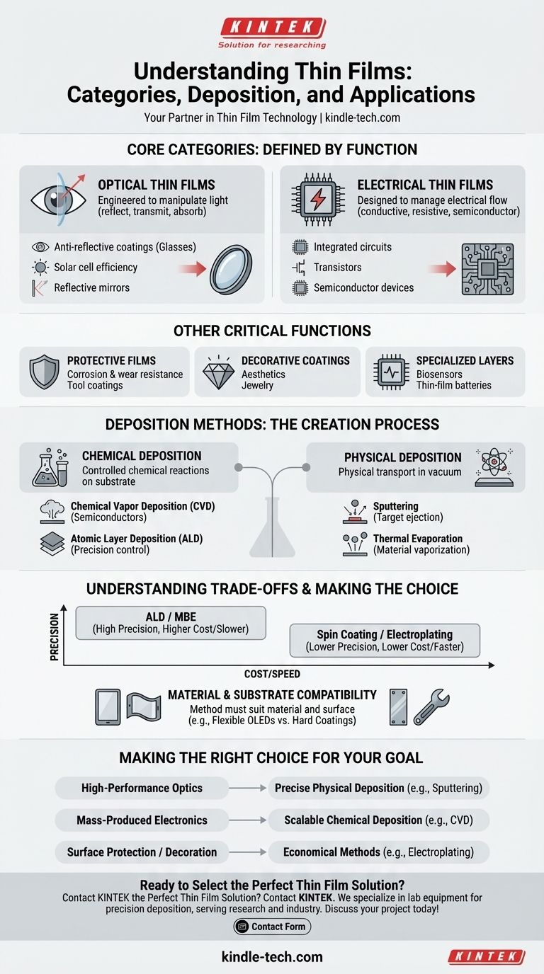
At their core, thin films are typically categorized by their primary function. While countless materials can be used, the two most common classifications are optical thin films, which are designed to manipulate light, and electrical thin films, which are engineered to manage the flow of electricity.
The "type" of a thin film is defined less by its material composition and more by its intended purpose. Understanding whether you need to control light, electricity, or physical properties is the first step in navigating this technology.
Functional Categories: The Primary Distinction
The most fundamental way to differentiate thin films is by what they are designed to accomplish. This functional distinction dictates the material choices, deposition methods, and ultimate application.
Optical Thin Films
These films are engineered to interact with light. Their purpose is to change the way a surface reflects, transmits, or absorbs different wavelengths.
Applications are widespread, including anti-reflective coatings on ophthalmic lenses, reflective layers in mirrors, and specialized coatings on solar cells to maximize light absorption.
Electrical Thin Films
This category focuses on controlling electrical properties. These films can be designed to be highly conductive, highly resistive (insulating), or to exhibit specific semiconductor behaviors.
They form the foundation of modern electronics, used to create the intricate layers within integrated circuits, transistors, and other semiconductor devices.
Other Critical Categories
While optical and electrical are the broadest classifications, many thin films are categorized by other essential functions.
These include protective films for corrosion and wear resistance on tools, decorative coatings on jewelry, and specialized layers for biosensors or thin-film batteries.
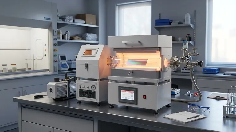
How Thin Films Are Made: A Look at Deposition
The properties of a thin film are inextricably linked to how it is created. The process, known as deposition, involves applying a material layer by layer onto a substrate, sometimes down to a single layer of atoms.
Chemical Deposition
These methods use controlled chemical reactions to build the film on a surface. The precursor materials react to form the desired compound, which then deposits onto the substrate.
Common techniques include Chemical Vapor Deposition (CVD), widely used in the semiconductor industry, and Atomic Layer Deposition (ALD), which offers exceptionally precise control.
Physical Deposition
These methods use physical or mechanical means to transport the film material onto the substrate. This often occurs in a vacuum environment.
Key examples are sputtering, where atoms are ejected from a target material, and thermal evaporation, where a material is heated until it vaporizes and condenses on the substrate.
Understanding the Trade-offs
The choice of deposition method is a critical decision with significant trade-offs. There is no single "best" method; the ideal choice depends entirely on the desired outcome and constraints.
Precision vs. Cost
Methods like Atomic Layer Deposition (ALD) and Molecular Beam Epitaxy (MBE) offer unparalleled precision, allowing for the construction of films one atomic layer at a time. This control comes at the cost of speed and expense.
Conversely, methods like spin coating or electroplating can be much faster and more cost-effective for larger areas but offer less control over the film's structure and thickness.
Material and Substrate Compatibility
Not all methods work for all materials. The chosen technique must be compatible with both the material being deposited and the substrate it is being applied to.
For example, depositing polymer compounds for flexible OLED displays requires different methods and conditions than creating hard, wear-resistant coatings on metal tools.
Making the Right Choice for Your Goal
Selecting the appropriate thin film technology begins with clearly defining your primary objective.
- If your primary focus is high-performance optics: You will likely need precise physical deposition methods like sputtering or evaporation to create specific multi-layer structures.
- If your primary focus is mass-produced electronics: Scalable chemical deposition methods like CVD are the industry standard for creating the complex layers in semiconductor devices.
- If your primary focus is surface protection or decoration: More economical and robust methods like electroplating or sputtering are often the most practical choice.
Ultimately, navigating the world of thin films is a process of matching a specific function to the most effective creation method for the task.
Summary Table:
| Category | Primary Function | Common Applications |
|---|---|---|
| Optical Thin Films | Manipulate light (reflect, transmit, absorb) | Anti-reflective coatings, solar cells, mirrors |
| Electrical Thin Films | Control electrical flow (conductive, resistive, semiconductor) | Integrated circuits, transistors, semiconductor devices |
| Protective/Decorative Films | Resist corrosion/wear or enhance appearance | Tool coatings, jewelry, biosensors |
Ready to select the perfect thin film solution for your application? KINTEK specializes in lab equipment and consumables for thin film deposition, serving research and industrial laboratories. Whether you need optical coatings, semiconductor layers, or protective films, our expertise ensures precision and reliability. Contact us today to discuss your project and discover how KINTEK can enhance your lab's capabilities!
Visual Guide