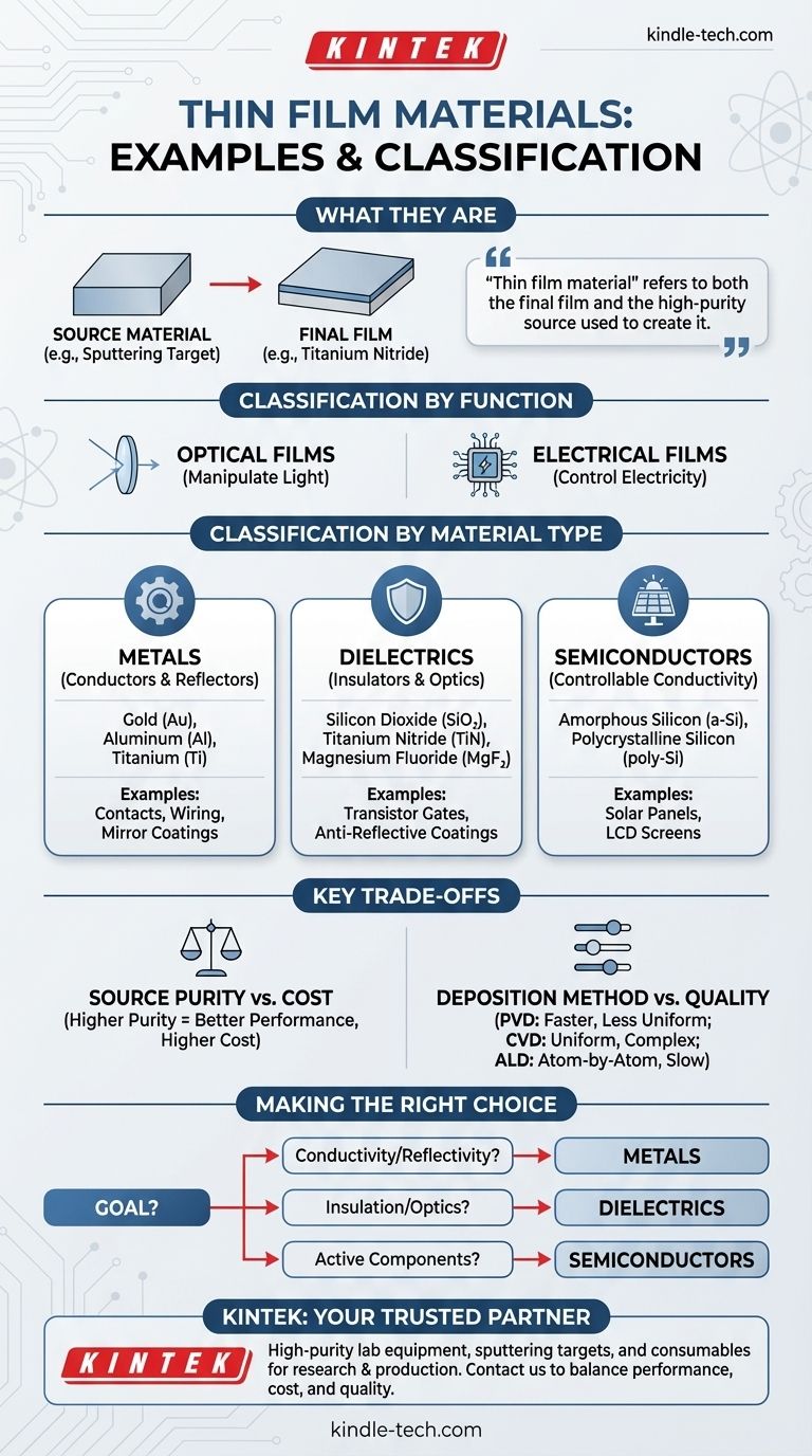
In short, common examples of thin film materials include metals like gold and aluminum, dielectrics such as silicon dioxide, and semiconductors like amorphous silicon. These materials are chosen for their specific properties and deposited in layers often no thicker than a few micrometers to alter the characteristics of a surface.
The term "thin film material" refers to two distinct but related concepts: the final material that forms the film (e.g., titanium nitride) and the high-purity source used to create it (e.g., a titanium sputtering target). Understanding this distinction is key to grasping how these microscopic layers enable modern technology.
How to Classify Thin Film Materials
The choice of a thin film material is never arbitrary; it is always dictated by the desired function of the final product. We can classify these materials by their application or their fundamental physical properties.
Classification by Function
The broadest classification is based on whether the film is designed to interact with light or electricity.
- Optical Films: These materials are used to manipulate light. They might be used for highly reflective coatings on mirrors, anti-reflective coatings on eyeglasses, or as components in solar cells and optical detectors.
- Electrical Films: These materials are used to control the flow of electricity. They serve as the foundational components for nearly all modern electronics, forming conductors, insulators, and semiconductor devices in integrated circuits.
Classification by Material Type
Drilling deeper, materials are chosen for these functions based on their inherent physical properties.
- Metals: These are excellent conductors of electricity and are often highly reflective. They are used for wiring in microchips and for creating reflective surfaces.
- Dielectrics: These are electrical insulators that do not conduct electricity well. They are used to isolate conductive layers from each other in circuits, for durable anti-scratch coatings, and to create anti-reflection layers on lenses.
- Semiconductors: These materials have electrical conductivity between that of a conductor and an insulator. This controllable conductivity makes them the foundation of transistors, diodes, and solar cells.
Common Examples of Thin Film Materials
Based on these classifications, here are some of the most common materials used in thin film applications.
Metallic Films
Metallic films are prized for their high conductivity and reflectivity.
- Gold (Au) & Platinum (Pt): Chosen for their excellent conductivity and resistance to corrosion, making them ideal for electrical contacts in high-performance electronics.
- Aluminum (Al): A cost-effective conductor and highly reflective material used for both integrated circuit wiring and mirror coatings.
- Titanium (Ti): Often used as a durable, biocompatible coating on medical implants or as an adhesion layer to help other films stick to a surface.
Dielectric (Insulating) Films
Dielectric films are essential for their insulating and optical properties.
- Silicon Dioxide (SiO₂): One of the most common insulators in the semiconductor industry, used to form the gate oxide layer in transistors that controls the flow of current.
- Titanium Nitride (TiN): An extremely hard ceramic material used as a durable, scratch-resistant coating on cutting tools and as a barrier layer in microchips.
- Magnesium Fluoride (MgF₂): Widely used as an anti-reflective coating on lenses and other optical components due to its low refractive index.
Semiconductor Films
Semiconductor films are the active components in most electronic devices.
- Amorphous Silicon (a-Si): A non-crystalline form of silicon used extensively in solar panels and thin-film transistors for LCD screens.
- Polycrystalline Silicon (poly-Si): Used in a wide variety of microelectronic devices, this form of silicon offers better performance than its amorphous counterpart.
Understanding the Key Trade-offs
The final properties of a thin film depend on both the material chosen and the method used to deposit it. This introduces critical trade-offs between performance, cost, and manufacturing speed.
Source Purity vs. Cost
The process begins with a high-purity source material, such as a sputtering target (a solid block of material) or a precursor gas. Higher purity leads to better, more predictable film performance, but it also significantly increases cost.
Deposition Method vs. Film Quality
The method used to deposit the film has a direct impact on its quality.
- Physical Vapor Deposition (PVD) methods like sputtering are versatile and relatively fast but can sometimes result in less uniform films compared to other methods.
- Chemical Vapor Deposition (CVD) creates highly uniform and pure films but often requires very high temperatures and complex precursor chemicals.
- Atomic Layer Deposition (ALD) offers unparalleled, atom-by-atom control over film thickness and uniformity, making it ideal for advanced microelectronics, but it is a very slow and expensive process.
Choosing the right combination of material and method is a constant balancing act between the ideal technical specifications and the practical constraints of a project budget and timeline.
Making the Right Choice for Your Goal
Your application's primary goal will determine the ideal material.
- If your primary focus is high conductivity or reflectivity: You will almost certainly need a metallic film like aluminum, gold, or copper.
- If your primary focus is electrical insulation or optical coating: Your best choice will be a dielectric material like silicon dioxide or magnesium fluoride.
- If your primary focus is creating active electronic components: You will need a semiconductor film, with silicon being the most dominant material in the industry.
Ultimately, the right thin film material is the one whose physical properties precisely match the function it needs to perform.
Summary Table:
| Material Type | Common Examples | Key Properties | Primary Applications |
|---|---|---|---|
| Metals | Gold (Au), Aluminum (Al), Titanium (Ti) | High conductivity, reflectivity, durability | Electrical contacts, wiring, mirror coatings, medical implants |
| Dielectrics | Silicon Dioxide (SiO₂), Titanium Nitride (TiN), Magnesium Fluoride (MgF₂) | Electrical insulation, hardness, anti-reflective | Transistor gates, scratch-resistant coatings, optical lenses |
| Semiconductors | Amorphous Silicon (a-Si), Polycrystalline Silicon (poly-Si) | Controllable conductivity | Solar panels, LCD screens, microelectronic devices |
Need the Right Thin Film Materials for Your Project?
Choosing the correct material—whether a high-purity metal, dielectric, or semiconductor—is critical to your application's success. The performance of your final product depends on both the material's intrinsic properties and the quality of the deposition process.
KINTEK is your trusted partner for all your thin film needs. We specialize in providing high-purity lab equipment and consumables, including sputtering targets and precursor materials, tailored for research and production environments. Our expertise ensures you get consistent, reliable results, whether you're developing advanced electronics, optical coatings, or durable surfaces.
Let us help you balance performance, cost, and quality.
Contact our experts today to discuss your specific requirements and discover how KINTEK's solutions can enhance your thin film applications.
Visual Guide