Looking beyond simple coatings, the future applications of thin films are set to power fundamental shifts in technology. We are moving toward active, intelligent systems such as flexible electronics, next-generation energy storage, and highly sensitive biomedical devices, all enabled by the ability to engineer material properties at the atomic level.
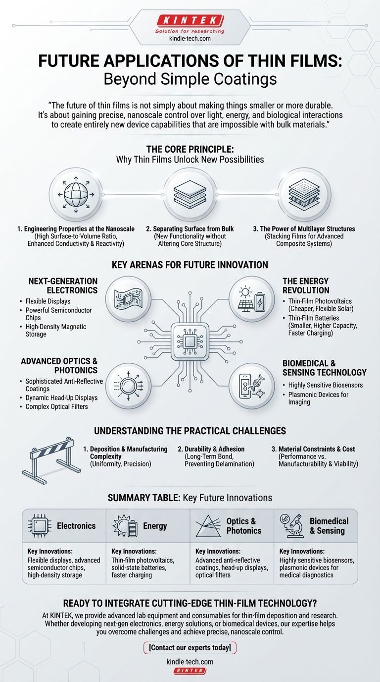
The future of thin films is not simply about making things smaller or more durable. It's about gaining precise, nanoscale control over light, energy, and biological interactions to create entirely new device capabilities that are impossible with bulk materials.
The Core Principle: Why Thin Films Unlock New Possibilities
To understand where the technology is heading, we must first understand why it is so powerful. The innovation isn't in the material itself, but in how its properties are transformed when reduced to a film just atoms thick.
Engineering Properties at the Nanoscale
When a material is reduced to a thin film, its surface-to-volume ratio increases dramatically. This fundamental shift alters its physical, chemical, and electrical properties, allowing us to create materials with enhanced conductivity, reactivity, or unique optical behaviors.
Separating Surface from Bulk
Thin films allow us to add new functionality to the surface of a material without altering its core structural properties. A flexible piece of plastic can be made into a circuit, and a strong steel tool can be made nearly frictionless, all with the application of a microscopic layer.
The Power of Multilayer Structures
The true potential is often realized by stacking different films to create a composite structure. By layering materials, we can create complex systems like advanced optical filters or semiconductor devices, combining properties that no single material possesses.
Key Arenas for Future Innovation
Current research and development point to several key sectors that thin films will revolutionize. These applications move far beyond simple protection and decoration into active, functional roles.
Next-Generation Electronics
The push for smaller, faster, and more flexible devices is entirely dependent on thin-film technology. This includes the development of flexible displays, more powerful semiconductor chips, and high-density magnetic storage media for computers.
The Energy Revolution
Thin films are at the heart of making energy generation and storage more efficient and accessible. Thin-film photovoltaic cells promise cheaper, more flexible solar panels, while thin-film batteries are key to creating smaller, higher-capacity, and faster-charging power sources for everything from phones to electric vehicles.
Advanced Optics and Photonics
The ability to precisely control light is a core strength of thin films. Future applications include more sophisticated anti-reflective coatings, dynamic head-up displays in vehicles, and complex optical filters used in telecommunications and scientific instruments.
Biomedical and Sensing Technology
The high surface area of thin films makes them incredibly sensitive. This is driving the future of biosensors capable of detecting minute quantities of biological markers for rapid medical diagnostics and the creation of plasmonic devices for advanced imaging.
Understanding the Practical Challenges
While the potential is immense, it's critical to recognize the engineering hurdles that define the cutting edge of thin-film research. The value of an application is always balanced against the difficulty of its implementation.
Deposition and Manufacturing Complexity
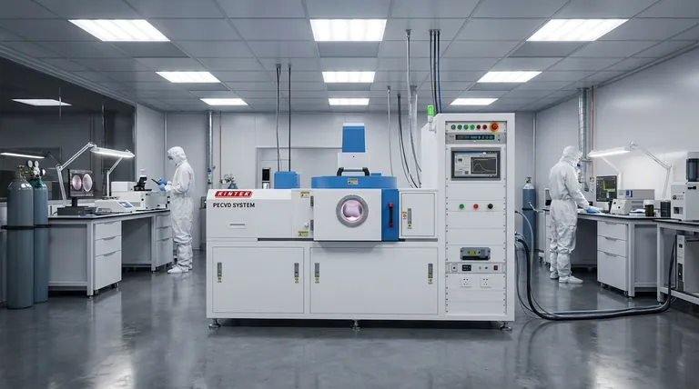
Creating a perfectly uniform, defect-free film—especially a complex multilayer structure—is a significant manufacturing challenge. The equipment is sophisticated, and the process requires extreme precision to ensure consistent performance.
Durability and Adhesion
A thin film is only as effective as its bond to the underlying material, or substrate. Ensuring long-term durability and preventing delamination (peeling) under physical or environmental stress is a primary focus of materials science.
Material Constraints and Cost
The ideal material for a specific property might be rare, expensive, or difficult to deposit as a thin film. The ongoing challenge is to find or engineer materials that balance peak performance with manufacturability and economic viability.
Making the Right Choice for Your Goal
The field is vast, so your focus should align with the fundamental capabilities that serve your objective.
- If your primary focus is energy efficiency and generation: Concentrate on advancements in thin-film photovoltaics and solid-state batteries, which promise higher efficiency and density.
- If your primary focus is consumer electronics: Investigate the development of flexible organic light-emitting diodes (OLEDs) and next-generation semiconductor materials.
- If your primary focus is industrial or aerospace applications: Prioritize research into novel wear-resistant, anti-corrosive, and thermal barrier coatings.
- If your primary focus is healthcare and diagnostics: Explore the rapidly growing field of thin-film biosensors and plasmonic devices for their unmatched sensitivity.
By understanding these core drivers, you can better anticipate the next wave of technological breakthroughs powered by thin films.
Summary Table:
| Application Area | Key Future Innovations Enabled by Thin Films |
|---|---|
| Electronics | Flexible displays, advanced semiconductor chips, high-density storage |
| Energy | Thin-film photovoltaics, solid-state batteries, faster charging |
| Optics & Photonics | Advanced anti-reflective coatings, head-up displays, optical filters |
| Biomedical & Sensing | Highly sensitive biosensors, plasmonic devices for medical diagnostics |
Ready to integrate cutting-edge thin-film technology into your research or product development?
At KINTEK, we specialize in providing the advanced lab equipment and consumables necessary for thin-film deposition and research. Whether you are developing next-generation electronics, more efficient energy solutions, or sensitive biomedical devices, our expertise can help you overcome manufacturing challenges and achieve precise, nanoscale control.
Contact our experts today to discuss how our solutions can accelerate your innovation in thin-film applications.
Visual Guide
Related Products
- Aluminized Ceramic Evaporation Boat for Thin Film Deposition
- Tungsten Evaporation Boat for Thin Film Deposition
- Electron Beam Evaporation Coating Oxygen-Free Copper Crucible and Evaporation Boat
- Molybdenum Tungsten Tantalum Evaporation Boat for High Temperature Applications
- Aluminum-Plastic Flexible Packaging Film for Lithium Battery Packaging
People Also Ask
- What is thin film deposition? Unlock Advanced Surface Engineering for Your Materials
- Why are high-purity ceramic boats used for lignin activation? Ensure Purity & Thermal Stability
- What is the chemical method for thin film deposition? Build Films from the Molecular Level Up
- What are the applications of thin films deposition? Unlock New Possibilities for Your Materials
- What are the alternatives to sputtering? Choose the Right Thin Film Deposition Method


