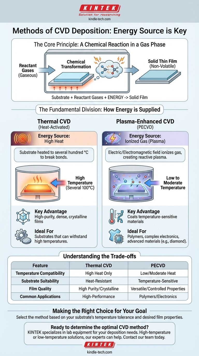
At its core, Chemical Vapor Deposition (CVD) is not a single method but a family of processes differentiated by how they supply energy to trigger a chemical reaction. The primary methods are categorized as either Thermally Activated CVD, which uses high heat, or Plasma-Enhanced CVD (PECVD), which uses an ionized gas to drive the reaction at lower temperatures.
The essential difference between CVD methods comes down to the energy source. Your choice between using high heat or an energized plasma directly determines the processing temperature, the types of materials you can coat, and the final properties of the deposited film.
The Core Principle: A Chemical Reaction in a Gas Phase
Before comparing methods, it's crucial to understand the fundamental process that all CVD techniques share. It is a method for creating a solid material, typically a thin film, from gaseous reactants.
The Substrate and Reactants
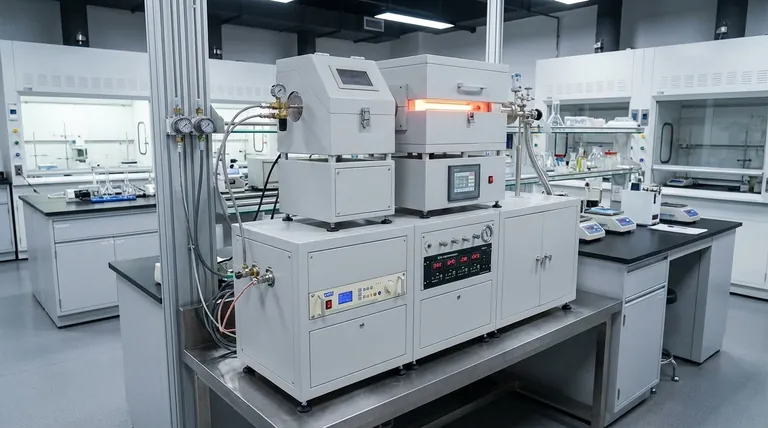
The process begins with a substrate, which is the material to be coated. This substrate is placed inside a reaction chamber under a controlled vacuum.
Volatile reactant gases, which contain the elements of the desired film, are then introduced into the chamber.
The Chemical Transformation
The goal is to provide enough energy to break down these reactant gases. This energy initiates a chemical reaction near the substrate surface.
The reaction is designed to produce a non-volatile, solid material that is chemically distinct from the original gases.
The Result: A Solid Thin Film
This newly formed solid material deposits onto the heated substrate, molecule by molecule, growing into a uniform and solid thin film. This film can enhance the substrate's durability, thermal properties, or reduce friction.
The Fundamental Division: How Energy is Supplied
The "method" of CVD is defined by the technique used to supply the energy needed for the chemical reaction. This is the most important distinction.
Method 1: Thermal CVD (Heat-Activated)
This is the classic approach. Energy is supplied simply by heating the substrate to a very high temperature, often several hundred degrees Celsius.
This intense heat provides the activation energy required for the reactant molecules to break their bonds and react on the substrate surface.
Method 2: Plasma-Enhanced CVD (PECVD)
PECVD uses a different energy source to avoid extremely high temperatures. Instead of relying solely on heat, it uses an electric or electromagnetic field to ionize the reactant gases, turning them into a plasma.
This energized plasma contains highly reactive ions and radicals that can facilitate the chemical reaction at much lower substrate temperatures. Specific techniques include microwave plasma and d.c. arc-jet plasmas, which are often used for creating advanced materials like synthetic diamond.
Understanding the Trade-offs
Choosing a CVD method involves balancing the requirements of your material, your substrate, and your desired outcome. There is no single "best" method.
Temperature and Substrate Compatibility
Thermal CVD's high heat requirement makes it unsuitable for temperature-sensitive substrates like plastics or certain electronic components, which could be damaged or destroyed.
PECVD is the solution for this problem. Its ability to run at lower temperatures allows for the successful coating of a much wider range of materials without causing thermal damage.
Film Quality and Control
The high temperatures in Thermal CVD often produce films that are highly pure, dense, and crystalline, which is ideal for many high-performance applications.
While PECVD is more versatile, the complex chemistry within the plasma can sometimes introduce impurities or result in a less ordered film structure. However, it also offers unique control over the film's properties.
Making the Right Choice for Your Goal
Your application's specific needs will dictate the correct CVD approach.
- If your primary focus is high-purity, crystalline films and your substrate can withstand high heat: Traditional Thermal CVD is often the most direct and effective method.
- If your primary focus is coating temperature-sensitive materials like polymers or complex electronics: Plasma-Enhanced CVD (PECVD) is the necessary choice to prevent damage.
- If your primary focus is growing advanced or specialized materials like synthetic diamond: Specific variants of PECVD, such as microwave plasma CVD, are the industry standard.
Ultimately, selecting the right CVD method is about choosing the right energy source to precisely control the creation of your material.
Summary Table:
| Method | Energy Source | Typical Temperature | Key Advantage | Ideal For |
|---|---|---|---|---|
| Thermal CVD | High Heat | High (Several 100°C) | High-purity, dense, crystalline films | Substrates that can withstand high temperatures |
| Plasma-Enhanced CVD (PECVD) | Ionized Gas (Plasma) | Low to Moderate | Coats temperature-sensitive materials | Polymers, complex electronics, advanced materials like diamond |
Ready to determine the optimal CVD method for your specific application?
At KINTEK, we specialize in providing the right lab equipment and consumables for your deposition needs. Whether you require the high-temperature precision of Thermal CVD systems or the versatile, low-temperature capabilities of PECVD, our experts can help you select the perfect solution to achieve superior thin film quality and protect your substrates.
Contact our team today to discuss your project and discover how KINTEK can enhance your laboratory's capabilities.
Visual Guide
Related Products
- Chemical Vapor Deposition CVD Equipment System Chamber Slide PECVD Tube Furnace with Liquid Gasifier PECVD Machine
- Customer Made Versatile CVD Tube Furnace Chemical Vapor Deposition Chamber System Equipment
- HFCVD Machine System Equipment for Drawing Die Nano-Diamond Coating
- Split Chamber CVD Tube Furnace with Vacuum Station Chemical Vapor Deposition System Equipment Machine
- Multi Heating Zones CVD Tube Furnace Machine Chemical Vapor Deposition Chamber System Equipment
People Also Ask
- What are the processes of vapor phase deposition? Understand CVD vs. PVD for Superior Thin Films
- What are the advantages of chemical vapor deposition? Achieve Superior Thin Films for Your Lab
- How are carbon nanotubes grown? Master Scalable Production with Chemical Vapor Deposition
- What is plasma enhanced chemical vapor deposition PECVD equipment? A Guide to Low-Temperature Thin Film Deposition
- Why is Chemical Vapor Deposition (CVD) equipment uniquely suited for constructing hierarchical superhydrophobic structures?


