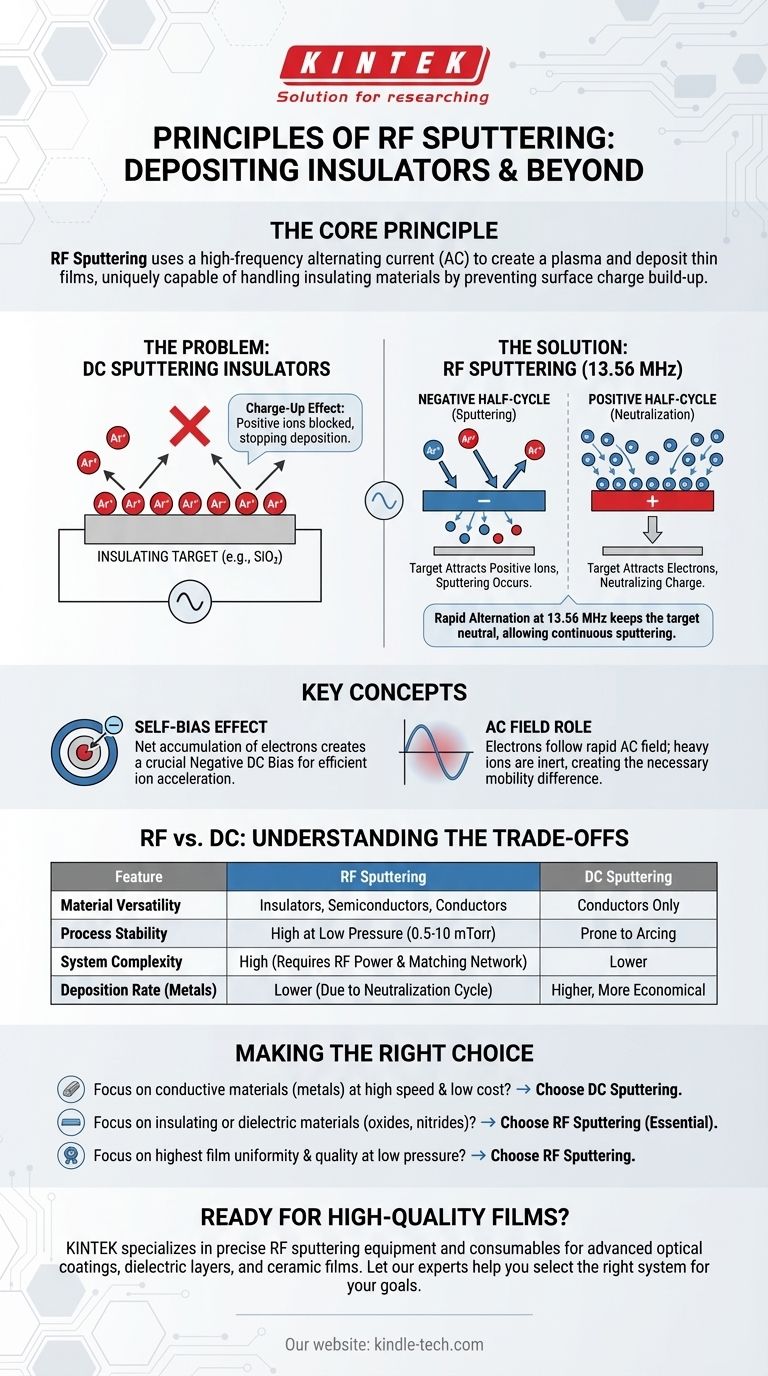
At its core, RF sputtering is a physical vapor deposition technique that uses a high-frequency alternating current to create a plasma and deposit thin films. Unlike its simpler counterpart, DC sputtering, RF sputtering is uniquely capable of depositing insulating (dielectric) materials. This is achieved by rapidly alternating the electrical potential on the target material, which prevents the build-up of surface charge that would otherwise halt the deposition process.
The fundamental challenge in sputtering non-conductive materials is the accumulation of positive charge on the target surface, which repels the very ions needed for deposition. RF sputtering solves this by using a high-frequency AC field that floods the target with electrons during one half of the cycle, effectively neutralizing the charge built up during the sputtering half-cycle.
The Fundamental Problem: Sputtering Insulators
The Limitation of DC Sputtering
Direct Current (DC) sputtering applies a constant negative voltage to a conductive target. This attracts positively charged ions (e.g., Argon) from the plasma, which strike the target with enough energy to dislodge, or "sputter," atoms that then deposit onto a substrate.
This method works perfectly for metals because the target can conduct away the positive charge delivered by the ions, maintaining the necessary negative potential.
The "Charge-Up" Effect
If you attempt to use DC sputtering with an insulating target (like quartz or alumina), the process fails almost instantly. The positive ions embed themselves in the surface, and because the material is an insulator, this positive charge cannot be neutralized.
This creates a positive surface layer that repels any further incoming positive ions from the plasma, effectively extinguishing the sputtering process before it begins. This is known as the "charge-up" effect.
How RF Sputtering Solves the Charge-Up Problem
The Role of the Alternating Current (AC) Field
RF sputtering replaces the DC power supply with a high-frequency AC source, operating at an industry-standard, federally allocated frequency of 13.56 MHz.
At this high frequency, the lightweight electrons in the plasma can respond almost instantly to the changing electric field, while the much heavier positive ions are too inert to follow the rapid oscillations. This difference in mobility is the key to the entire process.
The Negative Half-Cycle: Sputtering
During the part of the cycle where the target is negatively charged, it functions just like a DC target. It attracts the heavy, positive ions from the plasma, which bombard the surface and sputter away target material. This is the productive, deposition phase of the cycle.
The Positive Half-Cycle: Charge Neutralization
During the brief period when the target becomes positively charged, it immediately attracts a massive flux of highly mobile electrons from the plasma. This flood of electrons completely neutralizes the positive charge that accumulated on the insulating surface during the negative half-cycle.
Because this happens 13.56 million times per second, the target surface is effectively kept at a state of neutral potential, allowing the sputtering process to be sustained indefinitely.
The Critical Self-Bias Effect
Since electrons are far more mobile and responsive than ions, the target captures many more electrons during the positive cycle than it does ions during the negative cycle.
The result is a net accumulation of negative charge, causing the target to develop an overall negative DC bias even though it is powered by an AC source. This negative bias is crucial for ensuring that ions continue to be accelerated toward the target with enough energy for efficient sputtering.
Understanding the Trade-offs
Advantage: Unmatched Material Versatility
The primary advantage of RF sputtering is its ability to deposit any type of material, including insulators, semiconductors, and conductors. DC sputtering is strictly limited to conductive materials. This makes RF the go-to method for creating optical coatings, dielectric layers in electronics, and protective ceramic films.
Advantage: Process Stability at Low Pressure
The alternating field makes the process less prone to arcing compared to DC sputtering. Furthermore, RF systems are highly efficient at sustaining a plasma even at very low chamber pressures (0.5 to 10 mTorr). This results in fewer gas collisions and a longer mean free path for sputtered atoms, leading to higher-quality, denser films.
Disadvantage: System Complexity and Cost
RF sputtering systems are inherently more complex and expensive than their DC counterparts. They require a dedicated RF power supply and an impedance matching network to efficiently transfer power into the plasma. This added complexity often makes RF systems more suitable for smaller substrates or applications where film quality is paramount.
Disadvantage: Deposition Rate
For depositing simple metals, DC sputtering generally offers a higher deposition rate and is more economical. While RF can be highly efficient, the need to "spend" part of its cycle neutralizing charge means that for purely conductive targets, DC is often the faster choice.
Making the Right Choice for Your Goal
Selecting the correct sputtering technique depends entirely on the material you wish to deposit and your performance priorities.
- If your primary focus is depositing conductive materials (metals) at high speed and lower cost: DC sputtering is typically the more efficient and economical choice.
- If your primary focus is depositing insulating or dielectric materials (like oxides or nitrides): RF sputtering is the essential and non-negotiable technology to use.
- If your primary focus is achieving the highest film uniformity and quality, especially at low pressures: RF sputtering offers superior process control and stability for nearly any material.
Understanding this fundamental difference in charge management is the key to selecting the right tool for your thin-film deposition goals.
Summary Table:
| Principle | Function | Key Benefit |
|---|---|---|
| AC Field (13.56 MHz) | Rapidly alternates target potential | Prevents charge build-up on insulators |
| Negative Half-Cycle | Attracts positive ions for sputtering | Dislodges target atoms for deposition |
| Positive Half-Cycle | Attracts electrons for neutralization | Neutralizes surface charge |
| Self-Bias Effect | Creates a net negative DC bias | Ensures efficient ion acceleration |
Ready to deposit high-quality insulating films?
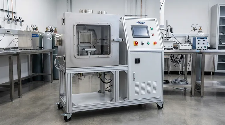
RF sputtering is essential for creating advanced optical coatings, dielectric layers, and ceramic films. KINTEK specializes in providing the precise lab equipment and consumables you need to master this technique.
Our experts can help you select the right RF sputtering system for your specific materials and performance goals, ensuring superior process stability and film quality.
Contact KINTEK today to discuss your thin-film deposition challenges and discover how our solutions can enhance your laboratory's capabilities.
Visual Guide
Related Products
- RF PECVD System Radio Frequency Plasma-Enhanced Chemical Vapor Deposition RF PECVD
- Horizontal High Temperature Graphite Vacuum Graphitization Furnace
- Spark Plasma Sintering Furnace SPS Furnace
- Automatic Laboratory Hydraulic Press for XRF & KBR Pellet Press
- Electron Beam Evaporation Coating Oxygen-Free Copper Crucible and Evaporation Boat
People Also Ask
- What is plasma CVD? Unlock Low-Temperature Thin Film Deposition for Sensitive Materials
- What is an example of PECVD? RF-PECVD for High-Quality Thin Film Deposition
- What is plasma chemical vapor deposition? A Low-Temperature Thin Film Coating Solution
- What is the role of RF-PECVD in VFG preparation? Mastering Vertical Growth and Surface Functionality
- How does plasma enhance CVD? Unlock Low-Temperature, High-Quality Film Deposition


