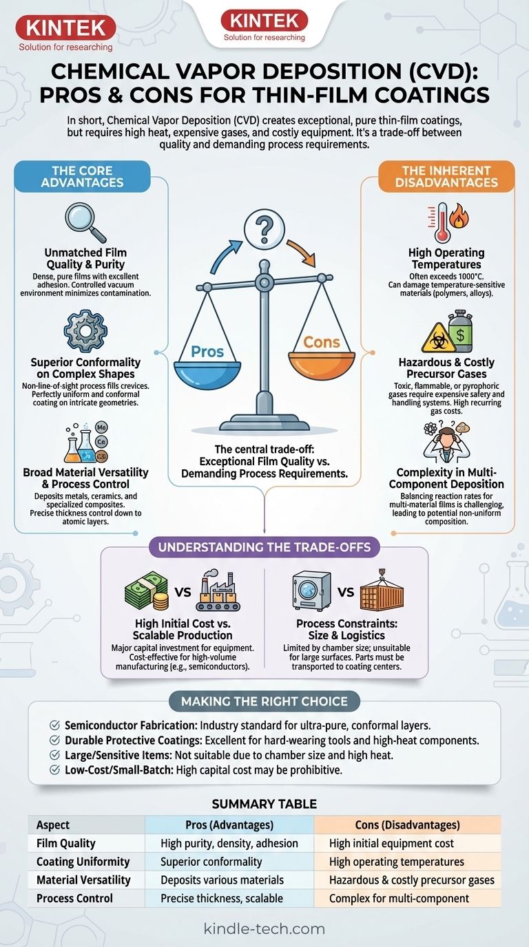
In short, Chemical Vapor Deposition (CVD) is a superior method for producing exceptionally pure, uniform, and durable thin-film coatings, even on complex surfaces. However, its advantages are balanced by significant drawbacks, including high operating temperatures that can damage sensitive materials, the use of potentially hazardous and expensive precursor gases, and high initial equipment costs.
The central trade-off of CVD is choosing between exceptional film quality and the demanding process requirements it entails. It is the gold standard for applications that can tolerate high heat and justify the investment, but it is impractical for temperature-sensitive substrates or low-budget, small-scale operations.
The Core Advantages of CVD
Chemical Vapor Deposition is not just one technique but a family of processes built on a powerful principle: building a solid film from the atoms up using chemical reactions from a gas phase. This foundation gives it several distinct advantages.
Unmatched Film Quality and Purity
CVD excels at creating films that are dense, pure, and have excellent adhesion to the substrate.
Because the process uses highly purified precursor gases in a controlled vacuum environment, sources of contamination are minimized. The resulting films are often near their theoretical density and exhibit exceptional purity.
Superior Conformality on Complex Shapes
One of the most significant advantages of CVD is its non-line-of-sight nature.
Imagine trying to paint a complex engine part with a spray can (a line-of-sight process); you will inevitably miss spots in crevices and on the backside. CVD, however, is more like filling the chamber with a steam that condenses evenly on every single exposed surface.
This allows it to deposit a perfectly uniform and conformal coating over intricate geometries, inside channels, and on irregularly shaped components—a feat impossible for many other deposition methods.
Broad Material Versatility and Process Control
The chemical nature of CVD makes it incredibly versatile. By changing the precursor gases, operators can deposit a vast range of materials, including metals, ceramics, and highly specialized composites.
This allows for fine-tuning the film's properties for specific applications, such as high hardness, corrosion resistance, or specific electrical characteristics. The process also provides precise control over film thickness, down to a single atomic layer, which is critical for manufacturing semiconductors and advanced electronics.
The Inherent Disadvantages of CVD
The same chemical reactions that give CVD its power also introduce its primary limitations. These challenges often revolve around heat, material safety, and process complexity.
High Operating Temperatures
Traditional CVD processes often require very high temperatures, sometimes exceeding 1000°C, to provide the necessary thermal energy to break down the precursor gases and initiate the chemical reaction on the substrate surface.
This high heat can damage or destroy temperature-sensitive materials, such as polymers or certain metal alloys, severely limiting the types of substrates that can be coated. While lower-temperature variants like Plasma-Enhanced CVD (PECVD) exist, they introduce their own set of complexities.
Hazardous and Costly Precursor Gases
The gases used in CVD are often toxic, flammable, or pyrophoric (igniting on contact with air). This necessitates sophisticated and expensive safety, handling, and exhaust abatement systems, which adds to the overall cost and operational complexity.
Furthermore, the high-purity specialty gases required can be a significant recurring expense, especially for advanced materials.
Complexity in Multi-Component Deposition
While CVD is excellent for depositing single materials, creating films with multiple components (e.g., specific alloys) can be difficult.
Each precursor gas has its own unique reaction rate and deposition characteristics. Co-depositing multiple materials requires balancing these variables perfectly, which can be a significant chemical engineering challenge, sometimes resulting in non-uniform composition.
Understanding the Trade-offs
Choosing CVD requires a clear understanding of its practical and financial implications. The decision is rarely about good versus bad, but about which set of compromises aligns with your project's goals.
High Initial Cost vs. Scalable Production
CVD systems represent a major capital investment. The vacuum chamber, gas delivery systems, heating elements, and safety equipment are expensive.
However, for high-volume manufacturing, CVD can become very cost-effective. Its high deposition rates, scalability, and high yield mean the cost-per-unit can be quite low once the initial investment is made, making it a mainstay in industries like semiconductor fabrication.
Process Constraints: Size and Logistics
CVD is constrained by the physical size of the vacuum chamber. This makes it impractical for coating very large surfaces.
Additionally, the process is almost always performed at a specialized coating center, meaning parts must be shipped, disassembled into individual components for coating, and then reassembled. This logistical overhead is not suitable for all applications.
Making the Right Choice for Your Goal
Your application's specific requirements should be the ultimate guide in deciding whether to use CVD.
- If your primary focus is semiconductor fabrication: CVD is an industry standard because its ability to create ultra-pure, ultra-thin, and perfectly conformal layers is non-negotiable.
- If your primary focus is creating durable protective coatings: CVD is an excellent choice for coating hard-wearing tools or engine components that can withstand high temperatures, as it produces highly adherent, dense films.
- If your primary focus is coating large items or temperature-sensitive materials: You must look for alternatives, as CVD's chamber size limitations and high heat requirements make it a poor fit.
- If your primary focus is low-cost R&D or small-batch production: The high capital expenditure of a CVD system may be prohibitive, and other methods might offer a better return on investment.
Ultimately, selecting a deposition technology is about matching the process's capabilities with your project's non-negotiable demands.
Summary Table:
| Aspect | Pros (Advantages) | Cons (Disadvantages) |
|---|---|---|
| Film Quality | High purity, density, and excellent adhesion | High initial equipment cost |
| Coating Uniformity | Superior conformality on complex shapes | High operating temperatures |
| Material Versatility | Deposits various materials (metals, ceramics) | Hazardous and costly precursor gases |
| Process Control | Precise thickness control, scalable for production | Complex for multi-component deposition |
Ready to Achieve Superior Thin-Film Coatings with Precision?
KINTEK specializes in providing advanced lab equipment and consumables for all your chemical vapor deposition needs. Whether you're in semiconductor fabrication, creating durable protective coatings, or conducting advanced materials research, our solutions deliver the exceptional purity, uniformity, and performance your laboratory demands.
Contact us today to discuss how our CVD expertise can enhance your process efficiency and material outcomes.
Visual Guide
Related Products
- Chemical Vapor Deposition CVD Equipment System Chamber Slide PECVD Tube Furnace with Liquid Gasifier PECVD Machine
- Microwave Plasma Chemical Vapor Deposition MPCVD Machine System Reactor for Lab and Diamond Growth
- 915MHz MPCVD Diamond Machine Microwave Plasma Chemical Vapor Deposition System Reactor
- Customer Made Versatile CVD Tube Furnace Chemical Vapor Deposition Chamber System Equipment
- HFCVD Machine System Equipment for Drawing Die Nano-Diamond Coating
People Also Ask
- What is the chemical vapor deposition growth process? Build Superior Thin Films from the Atom Up
- What is plasma enhanced chemical vapor deposition PECVD equipment? A Guide to Low-Temperature Thin Film Deposition
- Why is Chemical Vapor Deposition (CVD) equipment uniquely suited for constructing hierarchical superhydrophobic structures?
- How expensive is chemical vapor deposition? Understanding the True Cost of High-Performance Coating
- What are the processes of vapor phase deposition? Understand CVD vs. PVD for Superior Thin Films


