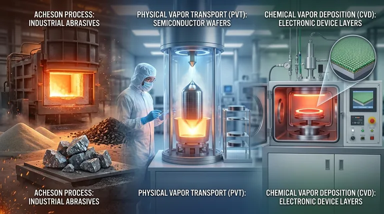
In short, silicon carbide (SiC) is synthesized through several distinct methods, each optimized for a specific end product and quality level. The primary commercial methods are the Acheson process for industrial-grade powders, Physical Vapor Transport (PVT) for high-purity single crystals used in electronics, and Chemical Vapor Deposition (CVD) for creating the active electronic layers on SiC wafers.
The choice of a silicon carbide synthesis method is fundamentally dictated by the end-use application. Low-cost, high-volume industrial uses rely on bulk powder synthesis, whereas high-performance electronics demand expensive, highly controlled crystal growth and film deposition techniques.
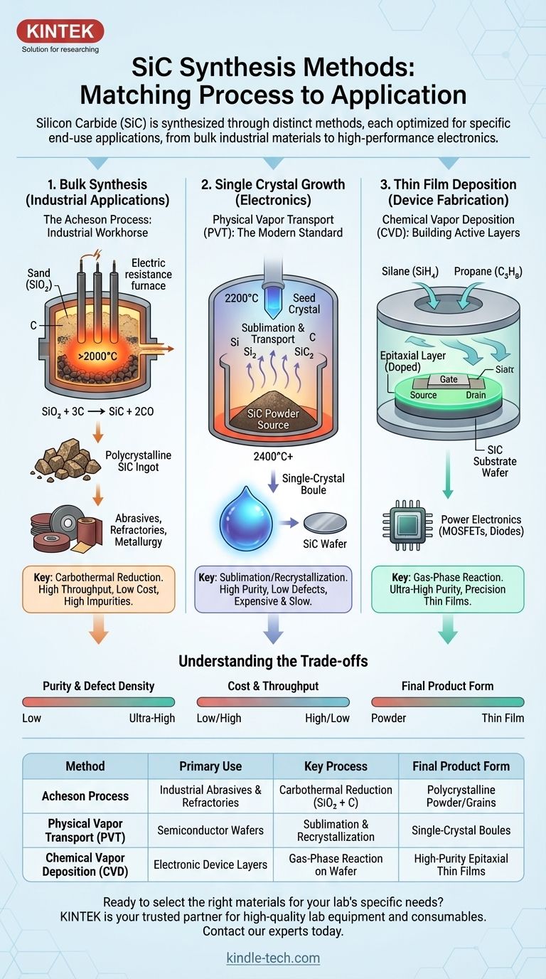
Bulk Synthesis for Industrial Applications
The original and most common method for producing SiC is designed for scale, not electronic-grade perfection. This material forms the backbone of the abrasives, refractory, and metallurgical industries.
The Acheson Process: The Industrial Workhorse
The Acheson process, developed in the 1890s, is a carbothermal reduction method. It involves heating a mixture of high-purity silica sand (SiO₂) and carbon-rich material, typically petroleum coke (C), in a large electric resistance furnace.
At temperatures exceeding 2000°C, the silica is reduced by the carbon, forming SiC and carbon monoxide gas. The result is a large, crystalline ingot of SiC.
This ingot is then cooled, crushed, and processed into grains and powders of varying sizes. Its primary use is for manufacturing grinding wheels, sandpaper, cutting tools, and as an additive in steel production.
Limitations of the Acheson Method
While highly effective for bulk production, the Acheson process yields material with relatively high impurity levels and a polycrystalline structure. This makes it entirely unsuitable for semiconductor applications, which require near-perfect single crystals.
Single Crystal Growth for Electronics
To create the SiC wafers needed for power electronics like MOSFETs and diodes, a far more precise method is required to grow large, single-crystal boules with minimal defects.
The Foundation: The Lely Method
The Lely method, developed in 1955, established the core principle of modern SiC crystal growth: sublimation. In this process, SiC powder is heated in a crucible to around 2500°C, causing it to sublimate (turn directly from a solid to a gas).
The SiC vapor then diffuses to a slightly cooler region within the crucible, where it recrystallizes into small, high-purity SiC platelets. While it produces very high-quality crystals, the process is difficult to control and does not produce large, usable wafers.
The Modern Standard: Physical Vapor Transport (PVT)
The Physical Vapor Transport (PVT) method, also known as the Modified Lely method, is the dominant commercial process for producing SiC wafers today. It refines the Lely concept for scalability and control.
In PVT, a high-purity SiC powder source is heated at the bottom of a sealed crucible. A precisely oriented SiC seed crystal is mounted at the top, which is kept at a slightly lower temperature.
The SiC source sublimates, and the gaseous species (Si, Si₂, C, SiC₂) travel up the temperature gradient to deposit onto the seed crystal. This deposition slowly grows a large, single-crystal boule that replicates the seed's crystal structure. This process can take over a week to grow one boule, which is then sliced into wafers.
Thin Film Deposition for Device Fabrication
The PVT-grown wafer is only a substrate—a foundation. The actual electronic components are built within an ultra-pure thin film grown on top of it.
Chemical Vapor Deposition (CVD): Building the Active Layers
Chemical Vapor Deposition (CVD) is used to grow a thin, precisely controlled epitaxial layer on the SiC substrate. This layer can be doped with other elements (like nitrogen or aluminum) to create the n-type and p-type regions that form transistors and diodes.
In a CVD reactor, precursor gases like silane (SiH₄) and a hydrocarbon (e.g., propane, C₃H₈) are flowed over the heated SiC wafer. The gases decompose and react on the hot surface, forming a new, perfect SiC crystal layer that exactly matches the substrate's crystal orientation.
Understanding the Trade-offs
Each method represents a compromise between cost, purity, and the final physical form of the material.
Purity and Defect Density
The Acheson process produces material sufficient for mechanical applications but is rife with impurities and crystal defects. In contrast, the PVT and CVD processes are conducted in highly controlled environments to achieve the ultra-high purity and low defect density essential for reliable electronic device performance.
Cost and Throughput
There is a massive cost disparity. The Acheson process is a relatively low-cost, high-throughput industrial method. PVT growth is extremely expensive due to the sophisticated equipment, immense energy consumption, and very slow growth rates. CVD is an additional high-cost, precision step required for every wafer.
Final Product Form
The method directly determines the output. The Acheson process creates polycrystalline chunks and powders. The PVT method is designed exclusively to produce large single-crystal boules. CVD is a deposition technique that only creates thin films on an existing substrate.
Making the Right Synthesis Choice
The "best" method is entirely dependent on the final goal.
- If your primary focus is industrial abrasives or metallurgical additives: The Acheson process is the only economically viable method for producing bulk SiC powder at scale.
- If your primary focus is producing wafers for power electronics: The Physical Vapor Transport (PVT) method is the non-negotiable industry standard for growing large, high-quality single-crystal boules.
- If your primary focus is fabricating semiconductor devices: Chemical Vapor Deposition (CVD) is the essential final step to grow the active, doped epitaxial layers on a PVT-grown SiC wafer.
Ultimately, the synthesis of silicon carbide is a story of matching a specific production method to a precise application, from industrial grit to the heart of advanced electronics.
Summary Table:
| Method | Primary Use | Key Process | Final Product Form |
|---|---|---|---|
| Acheson Process | Industrial Abrasives & Refractories | Carbothermal Reduction (SiO₂ + C) | Polycrystalline Powder/Grains |
| Physical Vapor Transport (PVT) | Semiconductor Wafers | Sublimation & Recrystallization | Single-Crystal Boules |
| Chemical Vapor Deposition (CVD) | Electronic Device Layers | Gas-Phase Reaction on Wafer | High-Purity Epitaxial Thin Films |
Ready to select the right materials for your lab's specific needs? Whether you're working on industrial materials R&D or developing next-generation semiconductor devices, KINTEK is your trusted partner for high-quality lab equipment and consumables. Our expertise ensures you have the right tools for your synthesis and analysis workflows. Contact our experts today to discuss how we can support your laboratory's goals with precision and reliability.
Visual Guide
Related Products
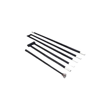
- Silicon Carbide SiC Thermal Heating Elements for Electric Furnace
- Silicon Carbide (SIC) Ceramic Sheet Wear-Resistant Engineering Advanced Fine Ceramics
- Silicon Carbide (SIC) Ceramic Plate for Engineering Advanced Fine Ceramics
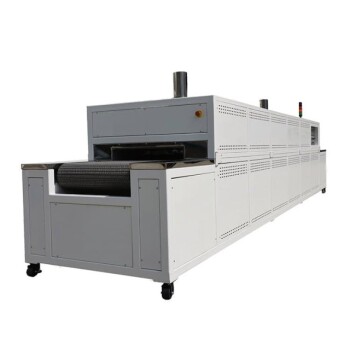
- Mesh belt controlled atmosphere furnace
- Large Vertical Graphite Vacuum Graphitization Furnace
People Also Ask
- What is silicon carbide rod heated to high temperature used as? A Premier Heating Element for Extreme Environments
- What is the function of the heating element in a furnace? The Engine of Your Thermal Process
- What is a silicon carbide heating element? Unlock Extreme Heat for Industrial Processes
- How long does a heating element last on the furnace? Understand Lifespan & Safety for Your System
- What is the maximum temperature for silicon carbide heating element? The Real Limit for Your High-Temp Furnace