In essence, an electron beam is a highly versatile tool used for an array of precise industrial and scientific tasks. Its applications range from fabricating the microscopic circuits in modern electronics via electron lithography to curing specialized inks and modifying the chemical structure of polymers and cable insulation.
The core value of electron beam technology lies in its ability to deliver a highly focused, precisely controlled stream of kinetic energy. This energy can be converted into intense, localized heat for material processing or used to initiate specific chemical reactions at a microscopic level.
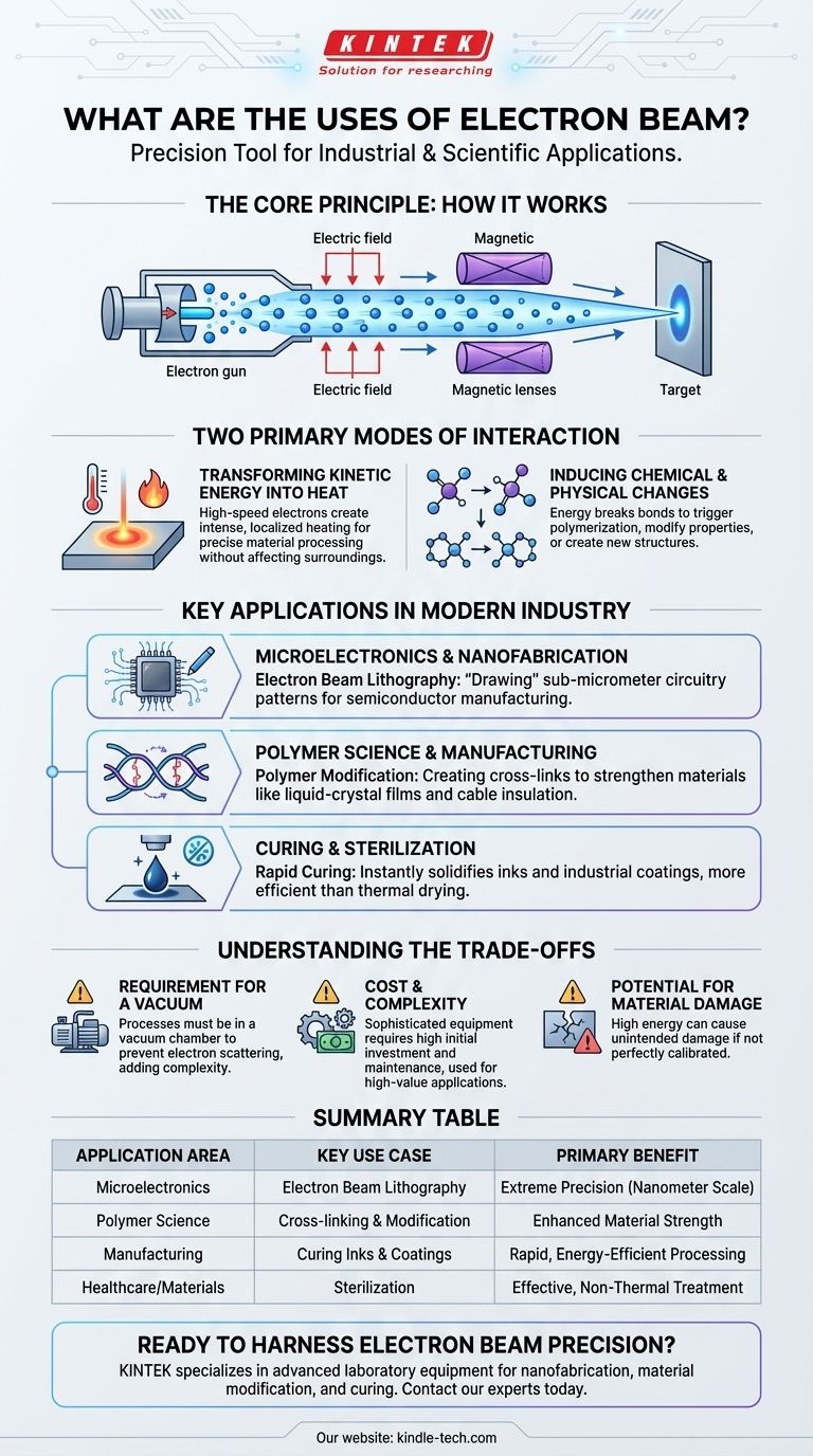
The Core Principle: How It Works
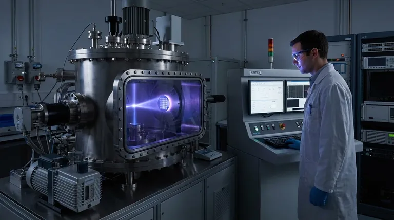
An electron beam is a stream of electrons accelerated to high speeds by an electric field and focused into a narrow beam using magnetic lenses. This concentration of high-energy particles is the source of its power and precision, enabling two primary modes of interaction with materials.
Transforming Kinetic Energy into Heat
When the high-speed electrons in the beam strike a material, their kinetic energy is rapidly converted into thermal energy.
This process creates an extremely high temperature at a very precise point, allowing for processes that require intense, localized heating without affecting the surrounding material.
Inducing Chemical and Physical Changes
The energy carried by the electrons is often sufficient to break chemical bonds within a material.
This capability is used to trigger polymerization (curing), create new molecular structures, or alter a material's properties, such as in the treatment of polymer films or cable insulation.
Key Applications in Modern Industry
The unique capabilities of electron beams have made them indispensable in several high-technology fields. Each application leverages the beam's precision and energy to achieve results that would be difficult or impossible with other methods.
Microelectronics and Nanofabrication
Electron beam lithography is a cornerstone of semiconductor manufacturing. The beam is used to "draw" extremely fine patterns—often on the sub-micrometer or nanometer scale—onto a sensitive material, which then becomes the blueprint for a microchip's circuitry.
Polymer Science and Manufacturing
In manufacturing, electron beams are used for the fabrication and modification of polymers. The energy from the beam can create cross-links between polymer chains, a process that strengthens materials like liquid-crystal films and the insulation on electrical cables.
Curing and Sterilization
The technology is also used for the rapid curing of color printing inks and industrial coatings. The electron beam initiates a chemical reaction that solidifies the liquid ink or coating almost instantly, a process that is faster and more energy-efficient than thermal drying.
Understanding the Trade-offs
While powerful, electron beam technology has specific operational requirements and limitations that are critical to understand.
Requirement for a Vacuum
Electrons are easily scattered by air molecules. Consequently, most electron beam processes must be conducted in a vacuum chamber to ensure the beam remains focused and delivers its energy efficiently to the target. This adds significant complexity and cost to the equipment.
Cost and Complexity
The systems required to generate, accelerate, and focus an electron beam are sophisticated and expensive. The high initial investment and maintenance costs mean this technology is typically reserved for high-value industrial or scientific applications where its precision is essential.
Potential for Material Damage
The same high energy that makes the beam so useful can also cause unintended damage to the substrate if not perfectly controlled. Precise calibration is necessary to ensure the energy is absorbed as intended without causing unwanted defects in the material.
Matching the Technology to Your Goal
To determine if electron beam technology is the right solution, it's crucial to align its capabilities with your primary objective.
- If your primary focus is extreme precision at a microscopic scale: Electron beam lithography is the definitive choice for fabricating nano-dimensional images and advanced semiconductor circuits.
- If your primary focus is rapid material modification without bulk heating: Electron beam curing and polymer cross-linking offer an efficient method for altering material properties on an industrial scale.
Ultimately, the power of an electron beam lies in its unparalleled control over energy at the microscopic level.
Summary Table:
| Application Area | Key Use Case | Primary Benefit |
|---|---|---|
| Microelectronics | Electron Beam Lithography | Extreme Precision (Nanometer Scale) |
| Polymer Science | Cross-linking & Modification | Enhanced Material Strength |
| Manufacturing | Curing Inks & Coatings | Rapid, Energy-Efficient Processing |
| Healthcare/Materials | Sterilization | Effective, Non-Thermal Treatment |
Ready to harness the precision of electron beam technology for your lab? KINTEK specializes in advanced laboratory equipment, including electron beam systems for research and industrial applications. Whether your goal is nanofabrication, material modification, or specialized curing, our expertise can help you achieve unparalleled control and efficiency. Contact our experts today to discuss how our solutions can accelerate your innovation.
Visual Guide
Related Products
- VHP Sterilization Equipment Hydrogen Peroxide H2O2 Space Sterilizer
- Laboratory High Pressure Steam Sterilizer Vertical Autoclave for Lab Department
- Laboratory High Pressure Horizontal Autoclave Steam Sterilizer for Lab Use
- Desktop Fast Laboratory Autoclave Sterilizer 35L 50L 90L for Lab Use
- Desktop Fast High Pressure Laboratory Autoclave Sterilizer 16L 24L for Lab Use
People Also Ask
- What does an e-beam do? A Versatile Tool for Welding, Sterilization, and Microfabrication
- What is the difference between UV sterilizer and autoclave? Sterilization vs. Disinfection Explained
- What is the standard time for sterilization? Optimize Your Process for Safety and Efficiency
- What are environmental impacts of biomass? Balancing Sustainability with Potential Harm
- How does electron beam sterilization work? Achieve Fast, Cold Sterilization for Medical Devices