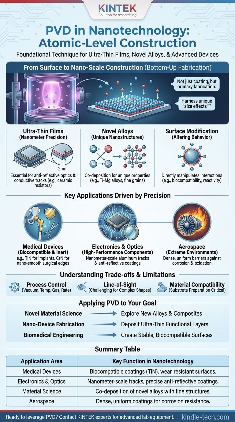
In nanotechnology, Physical Vapor Deposition (PVD) is a foundational technique used to construct materials and devices from the atomic level up. It enables the creation of ultra-thin films, coatings, and novel alloy compositions with precisely controlled properties that are impossible to achieve through traditional bulk manufacturing methods. This allows for the engineering of advanced medical implants, next-generation electronics, and high-performance components.
PVD is not merely a coating technology in the nano-realm; it is a primary fabrication tool. It gives researchers and engineers the power to build materials atom-by-atom, controlling their structure and function to harness the unique "size effects" that emerge at the nanoscale.
From Surface Coating to Nano-Scale Construction
While PVD is widely known for applying durable coatings on large objects like tools and engine parts, its role in nanotechnology is fundamentally different. It transitions from a surface treatment method to a bottom-up manufacturing process.
Creating Functional Ultra-Thin Films
PVD deposits material one atomic layer at a time. This precision is the key to creating films that are only a few nanometers thick, where the film's properties are dominated by its minute scale.
This is essential for applications like anti-reflective ceramic coatings on optics or the incredibly thin conductive aluminum tracks required for modern microelectronic circuits.
Engineering Novel Alloys and Materials
PVD allows for the co-deposition of multiple elements simultaneously. This process can create unique alloys, such as titanium-magnesium, that cannot be produced by conventional melting and casting (ingot metallurgy).
The resulting materials often exhibit fine grain sizes and extended solubilities, meaning the atoms are arranged in new, highly controlled nanostructures. This unlocks entirely new material properties.
Modifying the Surface of Nanomaterials
PVD techniques like magnetron sputtering can be used to apply a thin-film coating directly onto existing nanomaterials, such as nanoparticles.
This surface modification can fundamentally change the nanomaterial's behavior. A coating can make a particle biocompatible, alter its chemical reactivity, or change how it interacts with light, directly manipulating its "size effects."
Key Applications Driven by PVD's Precision
The ability to control matter at the nanoscale enables PVD to drive innovation across several high-tech fields.
Advanced Medical and Biocompatible Devices
PVD is critical for medical implants. Coatings like Titanium Nitride (TiN) are applied to prosthetics, creating a biocompatible and inert surface that prevents rejection by the body.
For surgical tools, coatings like Chromium Nitride (CrN) provide a nano-smooth, ultra-hard edge that maintains sharpness and resists corrosion, even through repeated high-temperature sterilization cycles.
Next-Generation Electronics and Optics
As electronic components shrink, the precision of PVD becomes non-negotiable. It is used to lay down the nanometer-scale aluminum tracks and ceramic resistors that form the basis of integrated circuits.
In optics, PVD is used to create anti-reflective coatings where the thickness of the film must be controlled with nanometer accuracy to effectively cancel out light waves.
Enhancing Performance in Extreme Environments
In aerospace, PVD coatings provide essential corrosion and oxidation resistance for components like gas turbine blades.
The dense, uniform nanostructure of a PVD coating creates a flawless barrier, preventing corrosive agents from finding microscopic weak points that would exist in a less-controlled coating.
Understanding the Trade-offs and Limitations
While powerful, PVD is a highly technical process with specific constraints that must be understood to be used effectively at the nanoscale.
The Critical Role of Process Control
Achieving nanoscale results requires meticulous control over process variables like vacuum pressure, temperature, gas composition, and deposition rate. PVD is not a single technique but a family of processes, and success depends on tuning these parameters perfectly.
Line-of-Sight Deposition
Most PVD processes are line-of-sight, meaning the coating material travels in a straight line from the source to the substrate. This can make it challenging to uniformly coat complex, three-dimensional nanostructures with high aspect ratios.
Material and Substrate Compatibility
The choice of materials is a key consideration. Not all materials can be easily vaporized and deposited, and the coating's adhesion is highly dependent on the substrate material it is being applied to. Substrate preparation is a critical step for successful nanocoating.
Applying PVD to Your Nanotechnology Goal
Your approach to PVD should be guided by your ultimate objective.
- If your primary focus is novel material science: Use PVD for co-deposition to explore and create new alloys and composites with unique nanostructures and properties unavailable through conventional means.
- If your primary focus is nano-device fabrication: Leverage PVD's precision for depositing the ultra-thin functional layers required for advanced electronics, sensors, and optical systems.
- If your primary focus is biomedical engineering: Employ PVD to create highly stable, biocompatible, and wear-resistant surfaces for implants, tools, and medical instruments.
Ultimately, PVD serves as a fundamental bridge, allowing us to translate atomic-level design into real-world technological advancements.
Summary Table:
| PVD Application Area | Key Function in Nanotechnology |
|---|---|
| Medical Devices | Creates biocompatible coatings (e.g., TiN) for implants and wear-resistant surfaces for surgical tools. |
| Electronics & Optics | Deposits nanometer-scale conductive tracks and anti-reflective coatings with precise thickness control. |
| Material Science | Enables co-deposition of novel alloys (e.g., Ti-Mg) with fine grain structures and extended solubility. |
| Aerospace Components | Provides dense, uniform nanostructured coatings for corrosion and oxidation resistance in extreme environments. |
Ready to leverage PVD for your nanotechnology projects? At KINTEK, we specialize in advanced lab equipment and consumables tailored for precise nanoscale fabrication. Whether you're developing next-generation medical implants, high-performance electronics, or novel materials, our expertise in PVD systems can help you achieve atomic-level control and unlock unique material properties. Contact our experts today to discuss how we can support your laboratory's innovation goals.
Visual Guide
Related Products
- HFCVD Machine System Equipment for Drawing Die Nano-Diamond Coating
- 915MHz MPCVD Diamond Machine Microwave Plasma Chemical Vapor Deposition System Reactor
- Vacuum Hot Press Furnace Machine for Lamination and Heating
- Laboratory Sterilizer Lab Autoclave Pulse Vacuum Lifting Sterilizer
- Laboratory Sterilizer Lab Autoclave Vertical Pressure Steam Sterilizer for Liquid Crystal Display Automatic Type
People Also Ask
- How do you calculate coating coverage? A Practical Guide to Accurate Material Estimation
- What machine is used to make lab-grown diamonds? Discover the HPHT & CVD Technologies
- How do CVD diamonds grow? A Step-by-Step Guide to Lab-Grown Diamond Creation
- What is direct current DC magnetron sputtering? A Guide to High-Quality Thin Film Deposition
- What is the process of coating deposition? A Step-by-Step Guide to Thin Film Engineering