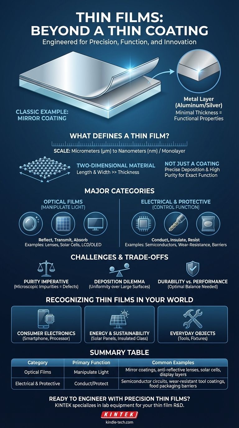
A classic example of a thin film is the reflective coating on a common household mirror. This extremely thin layer of metal, typically aluminum or silver, is deposited on the back of a sheet of glass to create a highly reflective surface. While it seems simple, this is a perfect illustration of a functional material whose properties are defined by its minimal thickness.
The key insight is that thin films are not just "thin coatings." They are highly engineered layers, often thinner than a wavelength of light, whose unique optical, electrical, and protective properties are fundamental to virtually all modern technology.
What Defines a Thin Film?
A thin film is a layer of material deposited onto a surface, known as a substrate. The defining characteristic is its extreme thinness, which fundamentally alters its physical properties compared to the same material in bulk form.
It's All About Scale
A thin film's thickness can range from a few micrometers (millionths of a meter) down to a single layer of atoms, known as a monolayer.
At this scale, the film is essentially a two-dimensional material. Its length and width are vast compared to its nearly non-existent thickness.
More Than Just a Coating
Unlike a simple layer of paint, thin films are created using precise deposition processes with high-purity materials.
This precision is necessary because the film's function—whether reflecting light, conducting electricity, or resisting corrosion—depends on its exact thickness, uniformity, and chemical purity.
The Major Categories of Thin Films
Thin films are generally grouped by their primary function. The two most common categories are those designed to interact with light (optical) and those designed for electrical or protective purposes.
Optical Films: Manipulating Light
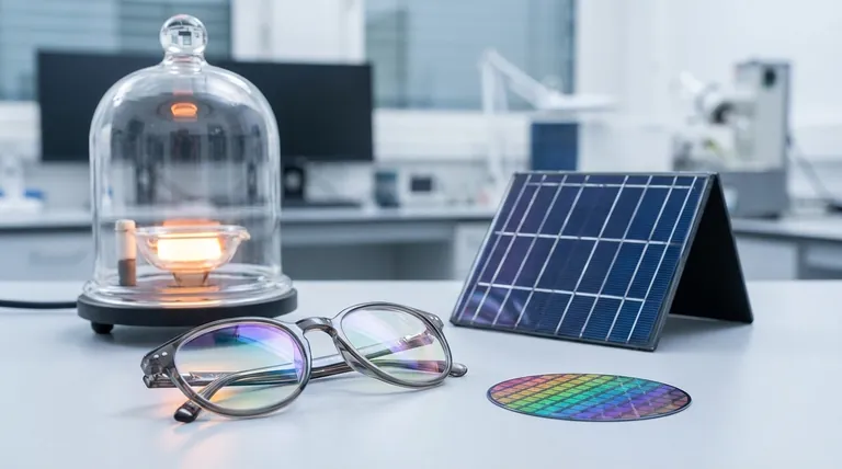
These films are designed to control how light is reflected, transmitted, or absorbed. The anti-reflective coating on your eyeglasses or camera lens is a perfect example.
Other applications include the reflective layers in mirrors, the light-absorbing layers in solar cells, and the multiple functional layers that make up modern LCD and OLED displays.
Electrical & Protective Films: Controlling Function
This broad category includes the microscopic layers of conductors, insulators, and semiconductors that form the integrated circuits inside a computer chip.
They also serve as protective barriers. A thin ceramic film on a drill bit provides wear resistance, while a specialized polymer film on food packaging prevents spoilage.
Understanding the Trade-offs and Challenges
Creating effective thin films is a complex engineering challenge. The properties that make them so useful also introduce significant manufacturing and durability constraints.
The Purity Imperative
Because the film is only a few atoms thick, even microscopic impurities can create defects that ruin its performance. This is why thin film production requires ultra-pure source materials and cleanroom environments.
The Deposition Dilemma
Applying a perfectly uniform layer just nanometers thick across a large surface is incredibly difficult. The process must be precisely controlled to ensure the film adheres properly to the substrate without cracking or peeling.
Durability vs. Performance
There is often a trade-off between a film's desired property (e.g., maximum light transmission) and its durability. A harder, more scratch-resistant coating might slightly reduce optical clarity, forcing engineers to find an optimal balance for the specific application.
How to Recognize Thin Films in Your World
By understanding their function, you can begin to identify the role of thin films in the technology and products you use every day.
- If your primary focus is consumer electronics: Think of the anti-glare and anti-fingerprint coatings on your smartphone screen and the intricate semiconductor layers inside its processor.
- If your primary focus is energy and sustainability: Look to the specialized layers in solar panels that convert light to electricity or the thermal insulation coatings on architectural glass that reduce heating costs.
- If your primary focus is everyday objects: Recognize the hard, wear-resistant coating on quality tools or the thin, decorative chrome layer on bathroom fixtures.
Once you know what to look for, you will find that our modern world is built upon these incredibly thin, high-performance layers.
Summary Table:
| Category | Primary Function | Common Examples |
|---|---|---|
| Optical Films | Manipulate Light | Mirror coatings, anti-reflective lenses, solar cells, display layers |
| Electrical & Protective Films | Conduct Electricity / Provide Protection | Semiconductor circuits, wear-resistant tool coatings, food packaging barriers |
Ready to Engineer Your Next Innovation with Precision Thin Films?
Thin films are the foundation of high-performance products, from advanced electronics to sustainable energy solutions. The key to success lies in precise deposition and material purity.
At KINTEK, we specialize in the lab equipment and consumables needed to develop and test these critical layers. Whether you're creating more efficient solar cells, durable protective coatings, or next-generation semiconductors, we provide the reliable tools to achieve the purity and uniformity your applications demand.
Let's build the future, one layer at a time. Contact our experts today to discuss your specific laboratory needs.
Visual Guide
Related Products
- Tungsten Evaporation Boat for Thin Film Deposition
- Aluminum-Plastic Flexible Packaging Film for Lithium Battery Packaging
- Thin-Layer Spectral Electrolysis Electrochemical Cell
- Lab Plastic PVC Calender Stretch Film Casting Machine for Film Testing
People Also Ask
- What is the process of thin film deposition? A Guide to PVD, CVD, and Coating Techniques
- What is the method of deposition of thin films? Choose the Right PVD or CVD Technique for Your Lab
- What method is used to make thin films? A Guide to Chemical and Physical Deposition
- What methods are used to deposit thin films? A Guide to PVD, CVD, and ALD Techniques
- What is a thin film evaporator? A Gentle Solution for Heat-Sensitive & Viscous Materials


