At its core, Chemical Vapor Deposition (CVD) is a highly controlled manufacturing process used to grow extremely thin, high-purity solid films onto a surface from a gaseous state. In semiconductor fabrication, this means precisely layering materials onto a silicon wafer. Reactive precursor gases are introduced into a vacuum chamber where they undergo a chemical reaction, decompose, and bond to the wafer’s surface, building the integrated circuit one atomic layer at a time.
Chemical Vapor Deposition isn't simply a coating technique; it is the fundamental architectural process for building a microchip. It uses controlled chemical reactions to construct the essential insulating, semiconducting, and conductive layers that define all modern electronic devices.

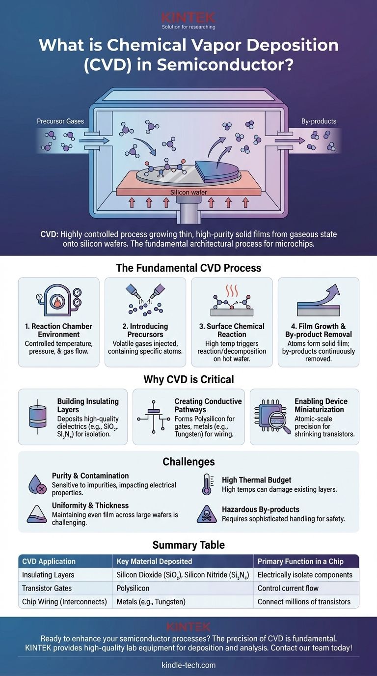
The Fundamental CVD Process: From Gas to Solid Film
To understand CVD's importance, we must first understand its mechanics. The process transforms gaseous ingredients into a solid, functional part of a microchip through a few critical steps.
The Reaction Chamber Environment
The entire process takes place inside a sealed deposition chamber. Conditions within this chamber, such as temperature, pressure, and gas flow, are controlled with extreme precision. The substrate, typically a silicon wafer, is placed inside and heated.
Introducing the Precursors
One or more volatile gases, known as precursors, are injected into the chamber. These gases contain the specific atoms required for the desired film—for example, to create a silicon dioxide film, precursors containing silicon and oxygen are used.
The Surface Chemical Reaction
The high temperature of the wafer provides the energy needed to trigger a chemical reaction. The precursor gases react or decompose directly on the hot wafer surface, breaking their chemical bonds and depositing the desired solid material.
Film Growth and By-product Removal
As the atoms deposit onto the surface, they form a thin, dense, and solid film. This layer builds up over time to a precisely controlled thickness. Any unwanted gaseous by-products from the reaction are continuously removed from the chamber by a vacuum system.
Why CVD is Critical for Semiconductor Manufacturing
CVD is one of the most widely used technologies in the semiconductor industry because it provides the control needed to build complex, microscopic structures. It is not used for just one purpose, but for creating several distinct types of essential layers.
Building the Insulating Layers
Microscopic components on a chip must be electrically isolated from one another to prevent short circuits. CVD is used to deposit high-quality insulating (dielectric) films like silicon dioxide (SiO₂) and silicon nitride (Si₃N₄) to serve this exact purpose.
Creating Conductive and Semiconductive Pathways
The process is also essential for depositing polysilicon, a key material used to form the "gate" of a transistor that turns it on and off. Other CVD variations are used to deposit metallic films, like tungsten, which act as the wiring that connects millions of transistors together.
Enabling Device Miniaturization
The power of CVD lies in its precision. It allows engineers to deposit films that are perfectly uniform and exceptionally thin, often just a few nanometers thick. This atomic-scale control is what makes it possible to continually shrink the size of transistors, making devices more powerful and cost-effective.
Understanding the Trade-offs and Challenges
While powerful, CVD is a complex process with inherent engineering challenges that must be meticulously managed.
Purity and Contamination Control
The entire process is extremely sensitive to impurities. Even trace amounts of unwanted elements in the precursor gases or the chamber can ruin the electrical properties of the film and render the microchip useless.
Uniformity and Thickness Control
Achieving a perfectly even film thickness across an entire 300mm silicon wafer is a significant challenge. Non-uniformity can lead to device performance variations across the chip, impacting yield and reliability.
High Thermal Budget
Many CVD processes require very high temperatures. This heat can potentially damage or alter other layers that have already been fabricated on the wafer, forcing engineers to carefully sequence the manufacturing steps.
Managing Hazardous By-products
The chemical reactions in CVD often produce volatile by-products that can be corrosive, flammable, or toxic. These materials require sophisticated handling and exhaust systems to ensure safety and environmental compliance.
Making the Right Choice for Your Goal
The specific variant of CVD chosen depends entirely on the desired material and its role within the integrated circuit.
- If your primary focus is creating high-quality insulators: Processes are optimized for depositing materials like silicon dioxide or silicon nitride with excellent dielectric properties to prevent electrical leakage.
- If your primary focus is forming transistor gates: Polysilicon CVD is used to create the gate structures that control the flow of current with extreme precision.
- If your primary focus is wiring the chip: Metallic CVD processes are employed to fill tiny trenches and vias, forming the complex network of interconnects that connect all the components.
Ultimately, mastering chemical vapor deposition is fundamental to fabricating the complex, multi-layered architecture of every modern microchip.
Summary Table:
| CVD Application | Key Material Deposited | Primary Function in a Chip |
|---|---|---|
| Insulating Layers | Silicon Dioxide (SiO₂), Silicon Nitride (Si₃N₄) | Electrically isolate components to prevent short circuits |
| Transistor Gates | Polysilicon | Form the gate structure that controls current flow in transistors |
| Chip Wiring (Interconnects) | Metals (e.g., Tungsten) | Create the conductive pathways that connect millions of transistors |
Ready to enhance your semiconductor or laboratory processes? The precision and control of CVD are fundamental to advanced manufacturing. KINTEK specializes in high-quality lab equipment and consumables, providing the reliable tools you need for deposition, material analysis, and more. Let our experts help you achieve superior results. Contact our team today to discuss your specific laboratory requirements!
Visual Guide
Related Products
- CVD Diamond Dressing Tools for Precision Applications
- Multi Heating Zones CVD Tube Furnace Machine Chemical Vapor Deposition Chamber System Equipment
- CVD Diamond Domes for Industrial and Scientific Applications
- CVD Diamond for Thermal Management Applications
- Chemical Vapor Deposition CVD Equipment System Chamber Slide PECVD Tube Furnace with Liquid Gasifier PECVD Machine
People Also Ask
- What is CVD diamond? The Ultimate Guide to Lab-Grown Diamonds and Their Uses
- Does the chemical vapor deposition be used for diamonds? Yes, for Growing High-Purity Lab Diamonds
- What are the disadvantages of CVD diamonds? Understanding the trade-offs for your purchase.
- What color diamonds are CVD? Understanding the Process from Brown Tint to Colorless Beauty
- How long does it take to make synthetic diamonds? Discover the 6-8 Week Science Behind Lab-Grown Gems


