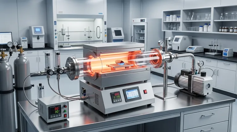
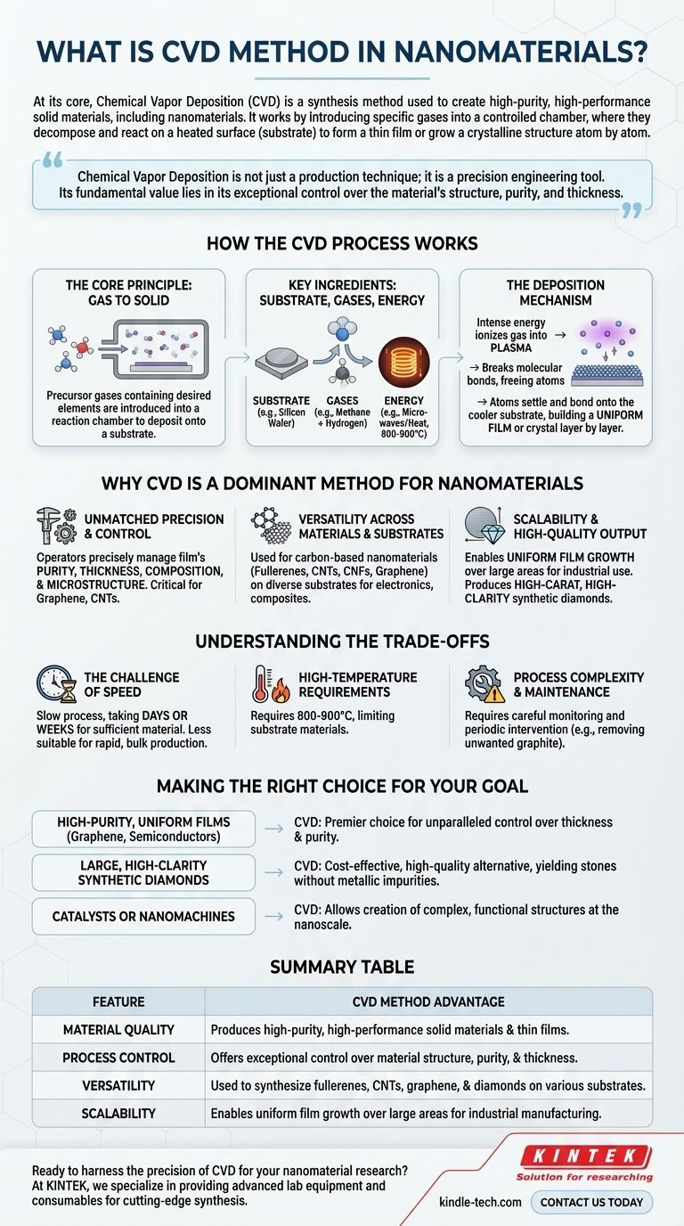
At its core, Chemical Vapor Deposition (CVD) is a synthesis method used to create high-purity, high-performance solid materials, including nanomaterials. The process works by introducing specific gases into a controlled chamber, where they decompose and react on a heated surface, known as a substrate, to form a thin film or grow a crystalline structure atom by atom.
Chemical Vapor Deposition is not just a production technique; it is a precision engineering tool. Its fundamental value lies in its exceptional control over the material's structure, purity, and thickness, making it indispensable for creating advanced nanomaterials where these properties dictate performance.
How the CVD Process Works
To understand the power of CVD, it's essential to grasp its fundamental mechanism. It is a process of controlled assembly, building a material from a gaseous state onto a solid foundation.
The Core Principle: Gas to Solid
The entire process hinges on a chemical reaction. Precursor gases, containing the elements you want to deposit, are introduced into a reaction chamber. These gases are then energized, causing them to break down and deposit the desired material onto the substrate.
Key Ingredients: Substrate, Gases, and Energy
The process begins by placing a substrate, such as a silicon wafer or a tiny diamond seed, inside a sealed chamber. A specific mixture of gases is then introduced. For creating synthetic diamonds or carbon nanotubes, this is often a carbon-rich gas like methane, mixed with hydrogen.
Finally, an energy source—typically microwaves, lasers, or a hot filament—heats the chamber to extremely high temperatures, often between 800°C and 900°C.
The Deposition Mechanism
This intense energy ionizes the gas, transforming it into a plasma. This breaks the molecular bonds in the gases, freeing the constituent atoms. For example, carbon atoms are stripped from the methane molecules.
These newly freed atoms then settle and bond onto the cooler substrate, slowly building up a uniform film or crystal layer by layer. This meticulous process ensures a highly ordered and pure final product.
Why CVD is a Dominant Method for Nanomaterials
CVD's unique capabilities make it a cornerstone technology for producing some of the most advanced materials used today.
Unmatched Precision and Control
The primary advantage of CVD is its fine-grained control. Operators can precisely manage the final film's purity, thickness, composition, and microstructure. This level of control is critical for nanomaterials like graphene and carbon nanotubes (CNTs), where even minor structural defects can drastically alter their electronic and mechanical properties.
Versatility Across Materials and Substrates
CVD is an incredibly versatile technique. It is used to synthesize a wide array of carbon-based nanomaterials, including fullerenes, CNTs, carbon nanofibers (CNFs), and graphene. Furthermore, it can be used to deposit these materials onto many different types of substrates, enabling its use in diverse applications from electronics to composite materials.
Scalability and High-Quality Output
The method allows for the growth of uniform films over large areas, which is crucial for industrial-scale manufacturing. In applications like synthetic diamond production, CVD produces high-carat, high-clarity diamonds (mostly VVS-VS) that are free of the metallic inclusions sometimes found in diamonds made with other methods.
Understanding the Trade-offs
No technology is without its limitations. Objectivity requires acknowledging where the CVD process involves compromises.
The Challenge of Speed
Precision comes at a price. The CVD process is often slow, with deposition sometimes taking days or even weeks to grow a sufficient amount of material. This makes it less suitable for applications requiring rapid, bulk material production.
High-Temperature Requirements
While CVD operates at low pressure, it requires significant heat. The high temperatures (800-900°C) limit the types of substrate materials that can be used without being damaged or melting.
Process Complexity and Maintenance
The CVD process is not a "set it and forget it" method. It often requires careful monitoring and periodic intervention. For instance, when growing diamonds, technicians must frequently stop the process to remove unwanted graphite that can form alongside the desired crystal.
Making the Right Choice for Your Goal
Applying CVD effectively means aligning its strengths with your specific objective.
- If your primary focus is high-purity, uniform films like graphene or coatings for semiconductors: CVD is the premier choice due to its unparalleled control over film thickness and purity.
- If your primary focus is producing large, high-clarity synthetic diamonds: CVD offers a cost-effective and high-quality alternative to high-pressure methods, yielding stones without metallic impurities.
- If your primary focus is manufacturing catalysts or nanomachines: The precision of CVD allows for the creation of complex, functional structures at the nanoscale.
Ultimately, CVD empowers engineers and scientists to design and build materials from the ground up, turning theoretical structures into tangible, high-performance applications.
Summary Table:
| Feature | CVD Method Advantage |
|---|---|
| Material Quality | Produces high-purity, high-performance solid materials and thin films. |
| Process Control | Offers exceptional control over material structure, purity, and thickness. |
| Versatility | Used to synthesize fullerenes, CNTs, graphene, and diamonds on various substrates. |
| Scalability | Enables uniform film growth over large areas for industrial manufacturing. |
Ready to harness the precision of CVD for your nanomaterial research?
At KINTEK, we specialize in providing the advanced lab equipment and consumables necessary for cutting-edge synthesis techniques like Chemical Vapor Deposition. Whether you are developing next-generation electronics with graphene or creating high-clarity synthetic diamonds, our expertise supports your quest for high-purity, high-performance materials.
Contact us today to discuss how our solutions can enhance your laboratory's capabilities. Let's build the future of materials science, together.
Visual Guide
Related Products
- Chemical Vapor Deposition CVD Equipment System Chamber Slide PECVD Tube Furnace with Liquid Gasifier PECVD Machine
- Customer Made Versatile CVD Tube Furnace Chemical Vapor Deposition Chamber System Equipment
- HFCVD Machine System Equipment for Drawing Die Nano-Diamond Coating
- Split Chamber CVD Tube Furnace with Vacuum Station Chemical Vapor Deposition System Equipment Machine
- Multi Heating Zones CVD Tube Furnace Machine Chemical Vapor Deposition Chamber System Equipment
People Also Ask
- What types of substrates are used in CVD to facilitate graphene films? Optimize Graphene Growth with the Right Catalyst
- What happens during deposition chemistry? Building Thin Films from Gaseous Precursors
- Why is Chemical Vapor Deposition (CVD) equipment uniquely suited for constructing hierarchical superhydrophobic structures?
- What are the processes of vapor phase deposition? Understand CVD vs. PVD for Superior Thin Films
- What is plasma enhanced chemical vapor deposition PECVD equipment? A Guide to Low-Temperature Thin Film Deposition


