At its core, Chemical Vapor Deposition (CVD) is a "bottom-up" nanofabrication method that builds nanomaterials atom by atom. It uses a chemical process where gaseous molecules, known as precursors, are introduced into a reaction chamber and decompose at high temperatures to form a high-quality, solid thin film on the surface of a substrate. This technique is extensively used to create a wide variety of carbon-based nanomaterials like graphene and carbon nanotubes.
The central principle of CVD is not merely depositing material, but "growing" it. By precisely controlling gas chemistry, temperature, and pressure, CVD enables the synthesis of highly ordered, chemically bonded nanomaterials directly onto a target surface with atomic-level precision.
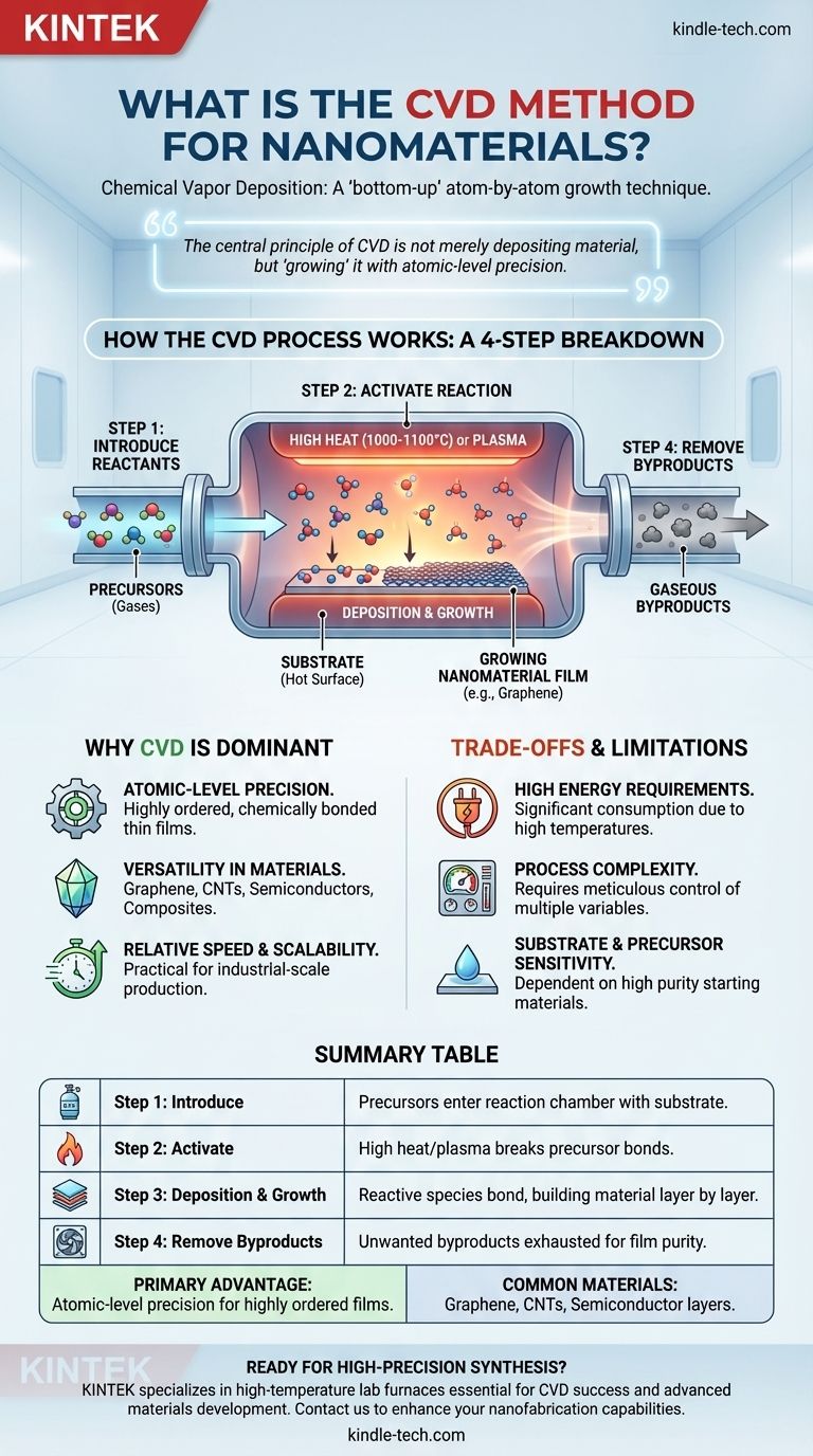
How the CVD Process Works: A Step-by-Step Breakdown
Understanding the CVD method is best done by breaking it down into its fundamental operational stages. Each step is critical for controlling the final properties of the nanomaterial.
Step 1: Introducing the Reactants
The process begins by feeding a precisely controlled mixture of reactive gases (precursors) into a sealed reaction chamber. This chamber contains a carefully prepared solid material called a substrate, which is the surface where the nanomaterial will grow.
Step 2: Activating the Reaction
For the chemical reaction to occur, the precursor gases need to be activated. This is typically achieved by heating the substrate to extremely high temperatures, often between 1000°C and 1100°C. This thermal energy breaks the chemical bonds in the precursor gases, creating reactive species. Other methods, such as plasma, can also be used for activation.
Step 3: Deposition and Growth
The activated, reactive gas species then travel and adsorb onto the hot substrate surface. Here, a series of chemical reactions occur, causing the desired atoms to bond with the substrate and with each other. This results in the deposition and growth of a solid thin film, building the nanomaterial one atomic layer at a time.
Step 4: Removing the Byproducts
The chemical reactions that form the solid material also create unwanted gaseous byproducts. These byproducts are continuously removed from the reaction chamber through an exhaust system to ensure the purity and quality of the final deposited film.
Why CVD is a Dominant Nanofabrication Technique
CVD is not just one method among many; its unique advantages make it a cornerstone of modern materials science, particularly for high-performance applications.
Atomic-Level Precision
The primary advantage of CVD is its ability to create chemically bonded thin films with exceptional control. Because the material grows atom by atom, the resulting structures are highly ordered and precise, which is crucial for fabricating materials like graphene or complex semiconductor layers.
Versatility in Materials
CVD is an incredibly versatile technique. It is the go-to method for synthesizing a range of advanced carbon nanomaterials, including:
- Graphene
- Carbon Nanotubes (CNTs)
- Carbon Nanofibers (CNFs)
- Fullerenes
Beyond carbon, specialized CVD techniques are used to grow intricate crystalline layers for the semiconductor industry and to create various composite material films.
Relative Speed and Scalability
Compared to many other nanofabrication techniques that operate on a smaller scale, CVD can be faster and more easily scaled for industrial production. This makes it a practical choice for producing materials in commercially viable quantities.
Understanding the Trade-offs and Limitations
While powerful, the CVD process is not without its challenges. A clear understanding of its limitations is essential for successful implementation.
High Energy Requirements
The high temperatures required for thermal CVD translate directly to significant energy consumption. This can make the process costly and presents an engineering challenge for maintaining temperature uniformity over large substrates.
Process Complexity
Successful CVD requires meticulous control over multiple variables simultaneously. Gas flow rates, chamber pressure, and substrate temperature must be precisely regulated, as even small deviations can dramatically impact the quality and consistency of the final nanomaterial.
Substrate and Precursor Sensitivity
The outcome of the CVD process is highly dependent on the quality of the starting materials. The substrate surface must be impeccably clean and properly prepared, and the precursor gases must be of high purity to avoid incorporating unwanted atoms into the growing film.
Making the Right Choice for Your Goal
Selecting CVD depends entirely on the desired properties of the final material and the scale of production.
- If your primary focus is high-purity crystalline films (like graphene or semiconductors): CVD is an exceptional choice due to its precise, layer-by-layer growth that yields superior structural quality.
- If your primary focus is producing large quantities of carbon nanotubes (CNTs): CVD offers a scalable and relatively fast manufacturing method compared to other synthesis techniques like arc discharge or laser ablation.
- If your primary focus is creating advanced composite materials: CVD is highly effective for infiltrating existing fabric structures or depositing functional coatings onto complex surfaces.
Ultimately, Chemical Vapor Deposition empowers engineers and scientists to construct advanced materials from the atoms up, enabling the creation of next-generation electronics, composites, and nanomachines.
Summary Table:
| CVD Process Stage | Key Function |
|---|---|
| Step 1: Introduce Reactants | Precursor gases enter the reaction chamber containing a substrate. |
| Step 2: Activate Reaction | High heat (1000-1100°C) or plasma breaks precursor bonds. |
| Step 3: Deposition & Growth | Reactive species adsorb and bond to the substrate, building the material layer by layer. |
| Step 4: Remove Byproducts | Unwanted gaseous byproducts are exhausted to ensure film purity. |
| Primary Advantage | Atomic-level precision for highly ordered, chemically bonded films. |
| Common Materials | Graphene, Carbon Nanotubes (CNTs), Semiconductor layers. |
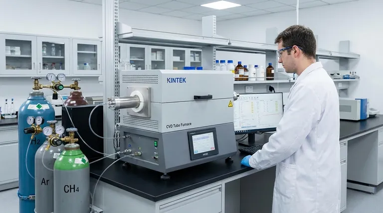
Ready to integrate high-precision nanomaterial synthesis into your research? The controlled environment of a CVD furnace is critical for success. KINTEK specializes in high-temperature lab furnaces and equipment essential for advanced materials development. Our expertise supports laboratories in achieving the precise temperature control and process consistency required for synthesizing graphene, CNTs, and other nanomaterials. Contact us today to discuss how our solutions can enhance your nanofabrication capabilities. Get in touch via our Contact Form
Visual Guide
Related Products
- HFCVD Machine System Equipment for Drawing Die Nano-Diamond Coating
- Microwave Plasma Chemical Vapor Deposition MPCVD Machine System Reactor for Lab and Diamond Growth
- Cylindrical Resonator MPCVD Machine System Reactor for Microwave Plasma Chemical Vapor Deposition and Lab Diamond Growth
- CVD Diamond for Thermal Management Applications
- Laboratory CVD Boron Doped Diamond Materials
People Also Ask
- What types of substrates are used in CVD to facilitate graphene films? Optimize Graphene Growth with the Right Catalyst
- What is the chemical vapor deposition growth process? Build Superior Thin Films from the Atom Up
- What are the disadvantages and challenges of the HFCVD method? Overcome Growth Limits and Filament Issues
- Why is Chemical Vapor Deposition (CVD) equipment uniquely suited for constructing hierarchical superhydrophobic structures?
- How expensive is chemical vapor deposition? Understanding the True Cost of High-Performance Coating


