Knowledge What is deposition in nanotechnology? Build High-Performance Materials Atom by Atom
Author avatar

Tech Team · Kintek Solution

Updated 1 week ago

What is deposition in nanotechnology? Build High-Performance Materials Atom by Atom


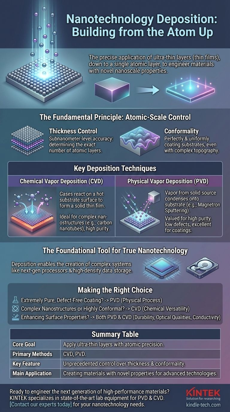
In the context of nanotechnology, deposition is the process of precisely applying an ultra-thin layer of material onto a surface, known as a substrate. These layers, or thin films, can be as thin as a single layer of atoms, allowing engineers to build materials from the ground up and endow them with entirely new properties.

Deposition moves beyond simply coating a surface; it is a foundational technique for engineering material properties at the atomic level. By controlling the exact placement of atoms and molecules, we can create high-performance materials that are impossible to produce using conventional bulk methods.

What is deposition in nanotechnology? Build High-Performance Materials Atom by Atom

The Fundamental Principle: Building From the Atom Up

At its core, nanotechnology deposition is about control. Unlike traditional coating methods like painting or electroplating, which apply thick, often imprecise layers, nano-deposition techniques are designed for atomic-scale precision.

From Bulk Material to Nanoscale Properties

The primary reason deposition is so critical is that materials behave differently at the nanoscale. A bulk material's properties (like color, conductivity, or strength) can change dramatically when it is structured as a thin film.

Deposition allows us to access and exploit these unique nanoscale properties. We can make a material more durable, scratch-resistant, transparent, or electrically conductive simply by structuring it as a precisely controlled thin film.

The Importance of the Substrate

The substrate is the base material or object onto which the thin film is deposited. It serves as the foundation for the new material being built. The interaction between the film and the substrate is critical to the final product's performance.

Achieving Unprecedented Control

Two concepts are central to the power of nanodeposition: thickness control and conformality.

Thickness control, often with subnanometer-level accuracy, means engineers can determine the exact number of atomic layers in the film. Conformality refers to the film's ability to perfectly and uniformly coat a substrate, even one with a complex, non-flat surface topography.

Key Deposition Techniques

Different methods are used to achieve deposition, each suited for different materials and outcomes. The two main families are Physical Vapor Deposition (PVD) and Chemical Vapor Deposition (CVD).

Chemical Vapor Deposition (CVD)

In CVD, precursor gases are introduced into a chamber where they react on the surface of the hot substrate. This chemical reaction forms a solid thin film on the substrate's surface.

This method is highly versatile and is capable of producing very pure, high-performance films, including complex nanostructures like carbon nanotubes.

Physical Vapor Deposition (PVD)

PVD techniques work by creating a vapor from a solid source material through physical means, which then condenses onto the substrate.

One common PVD method is magnetron sputtering. In this process, a target of the source material is bombarded with energized ions, which ejects atoms that then travel and deposit onto the substrate. This method is valued for creating films with high purity and a low level of defects.

Understanding the Trade-offs: Thin Films vs. True Nanotechnology

A nuanced debate exists within the field regarding deposition. Is the creation of a simple thin film truly considered "nanotechnology"?

The Core of the Debate

Some argue that if a thin film merely exhibits smaller-scale versions of its bulk properties, it doesn't represent true nanotechnology. The "true" goal, they contend, is the creation of complex devices and structures with novel functions, like nanomachines or intricate circuits.

The Reality: A Foundational Tool

While a simple film may not be a nanomachine, deposition techniques are the foundational tools that enable the creation of true nanotechnologies. They are the essential first step.

Without the ability to lay down atomically precise layers, it would be impossible to build the more complex systems that define the cutting edge of the field, such as next-generation processors and high-density data storage systems.

Making the Right Choice for Your Goal

The deposition method you choose depends entirely on the desired outcome for your material or device.

  • If your primary focus is creating an extremely pure, defect-free coating: PVD methods like magnetron sputtering are an excellent choice for their clean and controlled physical process.
  • If your primary focus is growing complex nanostructures or highly conformal layers: CVD offers the chemical versatility to build structures like carbon nanotubes from gaseous precursors.
  • If your primary focus is enhancing a bulk material's surface properties: Both PVD and CVD are powerful tools for adding durability, new optical qualities, or conductivity to a substrate.

Ultimately, deposition is the critical bridge that translates the science of the nanoscale into tangible, high-performance technologies.

Summary Table:

Aspect Key Detail
Core Goal Apply ultra-thin layers of material with atomic-scale precision.
Primary Methods Chemical Vapor Deposition (CVD), Physical Vapor Deposition (PVD).
Key Feature Unprecedented control over thickness and conformality.
Main Application Creating materials with novel properties for advanced technologies.

Ready to engineer the next generation of high-performance materials?

The precise control of nanoscale deposition is key to developing advanced electronics, durable coatings, and innovative optical devices. At KINTEK, we specialize in providing state-of-the-art lab equipment and consumables for your deposition needs, whether you're exploring new materials or scaling up production.

Our expertise in PVD and CVD systems can help you achieve the atomic-level precision your research demands. Contact our experts today to discuss how we can support your laboratory's nanotechnology goals.

Visual Guide

What is deposition in nanotechnology? Build High-Performance Materials Atom by Atom Visual Guide

Related Products

People Also Ask

Related Products

RF PECVD System Radio Frequency Plasma-Enhanced Chemical Vapor Deposition RF PECVD

RF PECVD System Radio Frequency Plasma-Enhanced Chemical Vapor Deposition RF PECVD

RF-PECVD is an acronym for "Radio Frequency Plasma-Enhanced Chemical Vapor Deposition." It deposits DLC (Diamond-like carbon film) on germanium and silicon substrates. It is utilized in the 3-12um infrared wavelength range.

HFCVD Machine System Equipment for Drawing Die Nano-Diamond Coating

HFCVD Machine System Equipment for Drawing Die Nano-Diamond Coating

The nano-diamond composite coating drawing die uses cemented carbide (WC-Co) as the substrate, and uses the chemical vapor phase method ( CVD method for short ) to coat the conventional diamond and nano-diamond composite coating on the surface of the inner hole of the mold.

Inclined Rotary Plasma Enhanced Chemical Vapor Deposition PECVD Equipment Tube Furnace Machine

Inclined Rotary Plasma Enhanced Chemical Vapor Deposition PECVD Equipment Tube Furnace Machine

Upgrade your coating process with PECVD coating equipment. Ideal for LED, power semiconductors, MEMS and more. Deposits high-quality solid films at low temps.

Chemical Vapor Deposition CVD Equipment System Chamber Slide PECVD Tube Furnace with Liquid Gasifier PECVD Machine

Chemical Vapor Deposition CVD Equipment System Chamber Slide PECVD Tube Furnace with Liquid Gasifier PECVD Machine

KT-PE12 Slide PECVD System: Wide power range, programmable temp control, fast heating/cooling with sliding system, MFC mass flow control & vacuum pump.

915MHz MPCVD Diamond Machine Microwave Plasma Chemical Vapor Deposition System Reactor

915MHz MPCVD Diamond Machine Microwave Plasma Chemical Vapor Deposition System Reactor

915MHz MPCVD Diamond Machine and its multi-crystal effective growth, the maximum area can reach 8 inches, the maximum effective growth area of single crystal can reach 5 inches. This equipment is mainly used for the production of large-size polycrystalline diamond films, the growth of long single crystal diamonds, the low-temperature growth of high-quality graphene, and other materials that require energy provided by microwave plasma for growth.

Customer Made Versatile CVD Tube Furnace Chemical Vapor Deposition Chamber System Equipment

Customer Made Versatile CVD Tube Furnace Chemical Vapor Deposition Chamber System Equipment

Get your exclusive CVD furnace with KT-CTF16 Customer Made Versatile Furnace. Customizable sliding, rotating, and tilting functions for precise reactions. Order now!

Cylindrical Resonator MPCVD Machine System Reactor for Microwave Plasma Chemical Vapor Deposition and Lab Diamond Growth

Cylindrical Resonator MPCVD Machine System Reactor for Microwave Plasma Chemical Vapor Deposition and Lab Diamond Growth

Learn about Cylindrical Resonator MPCVD Machine, the microwave plasma chemical vapor deposition method used for growing diamond gemstones and films in the jewelry and semi-conductor industries. Discover its cost-effective advantages over traditional HPHT methods.

Electron Beam Evaporation Coating Oxygen-Free Copper Crucible and Evaporation Boat

Electron Beam Evaporation Coating Oxygen-Free Copper Crucible and Evaporation Boat

Electron Beam Evaporation Coating Oxygen-Free Copper Crucible enables precise co-deposition of various materials. Its controlled temperature and water-cooled design ensure pure and efficient thin film deposition.

VHP Sterilization Equipment Hydrogen Peroxide H2O2 Space Sterilizer

VHP Sterilization Equipment Hydrogen Peroxide H2O2 Space Sterilizer

A hydrogen peroxide space sterilizer is a device that uses vaporized hydrogen peroxide to decontaminate enclosed spaces. It kills microorganisms by damaging their cellular components and genetic material.

Laboratory Sterilizer Lab Autoclave Vertical Pressure Steam Sterilizer for Liquid Crystal Display Automatic Type

Laboratory Sterilizer Lab Autoclave Vertical Pressure Steam Sterilizer for Liquid Crystal Display Automatic Type

Liquid crystal display automatic vertical sterilizer is a safe, reliable and automatic control sterilization equipment, which is composed of heating system, microcomputer control system and overheating and overvoltage protection system.

Anti-Cracking Press Mold for Lab Use

Anti-Cracking Press Mold for Lab Use

The anti-cracking press mold is a specialized equipment designed for molding various shapes and sizes of film using high pressure and electric heating.

High Performance Laboratory Freeze Dryer for Research and Development

High Performance Laboratory Freeze Dryer for Research and Development

Advanced laboratory freeze dryer for lyophilization, preserving sensitive samples with precision. Ideal for biopharmaceuticals, research & food industries.

Three-dimensional electromagnetic sieving instrument

Three-dimensional electromagnetic sieving instrument

KT-VT150 is a desktop sample processing instrument for both sieving and grinding. Grinding and sieving can be used both dry and wet. The vibration amplitude is 5mm and the vibration frequency is 3000-3600 times/min.

Benchtop Laboratory Freeze Dryer for Lab Use

Benchtop Laboratory Freeze Dryer for Lab Use

Premium benchtop laboratory freeze dryer for lyophilization, preserving samples with ≤ -60°C cooling. Ideal for pharmaceuticals & research.

Non Consumable Vacuum Arc Induction Melting Furnace

Non Consumable Vacuum Arc Induction Melting Furnace

Explore the benefits of Non-Consumable Vacuum Arc Furnace with high melting point electrodes. Small, easy to operate & eco-friendly. Ideal for laboratory research on refractory metals & carbides.

High Performance Laboratory Freeze Dryer

High Performance Laboratory Freeze Dryer

Advanced lab freeze dryer for lyophilization, preserving biological & chemical samples efficiently. Ideal for biopharma, food, and research.

Multi-Punch Rotary Tablet Press Mold Ring for Rotating Oval and Square Molds

Multi-Punch Rotary Tablet Press Mold Ring for Rotating Oval and Square Molds

The multi-punch rotary tablet press mold stands as a pivotal component in pharmaceutical and manufacturing industries, revolutionizing the process of tablet production. This intricate mold system comprises multiple punches and dies arranged in a circular fashion, facilitating rapid and efficient tablet formation.

Laboratory Vibratory Sieve Shaker Machine Slap Vibrating Sieve

Laboratory Vibratory Sieve Shaker Machine Slap Vibrating Sieve

KT-T200TAP is a slapping and oscillating sieving instrument for laboratory desktop use, with 300 rpm horizontal circular motion and 300 vertical slapping motions to simulate manual sieving to help sample particles pass through better.

Custom PTFE Teflon Parts Manufacturer for PTFE Buchner Funnel and Triangular Funnel

Custom PTFE Teflon Parts Manufacturer for PTFE Buchner Funnel and Triangular Funnel

The PTFE funnel is a piece of laboratory equipment used primarily for filtration processes, particularly in the separation of solid and liquid phases in a mixture. This setup allows for efficient and rapid filtration, making it indispensable in various chemical and biological applications.

Small Vacuum Heat Treat and Tungsten Wire Sintering Furnace

Small Vacuum Heat Treat and Tungsten Wire Sintering Furnace

The small vacuum tungsten wire sintering furnace is a compact experimental vacuum furnace specially designed for universities and scientific research institutes. The furnace features a CNC welded shell and vacuum piping to ensure leak-free operation. Quick-connect electrical connections facilitate relocation and debugging, and the standard electrical control cabinet is safe and convenient to operate.


Leave Your Message