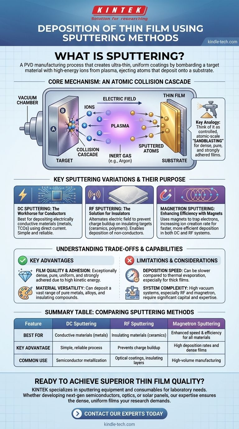
In short, sputtering is a manufacturing process that creates an ultra-thin coating on a surface. It works by bombarding a source material, known as the "target," with high-energy ions from a plasma. This atomic-level collision ejects atoms from the target, which then travel and deposit onto a nearby substrate—like a silicon wafer or optical lens—forming a highly uniform and durable thin film.
The key to understanding sputtering is to think of it not as painting, but as a controlled, atomic-scale "sandblasting." This high-energy physical process is what creates exceptionally dense, pure, and strongly adhered films, making it a cornerstone technique for high-performance electronics and optics.
The Core Mechanism: An Atomic Collision Cascade
Sputtering is a form of Physical Vapor Deposition (PVD). This means the material being deposited is physically transferred from a solid source to the substrate without undergoing a chemical reaction.
The Key Players: Target, Substrate, and Plasma
The process takes place in a vacuum chamber and involves three main components. The target is a block of the material you want to deposit. The substrate is the object you want to coat. The plasma, typically created from an inert gas like Argon, provides the high-energy ions for the bombardment.
How It Works: The Sputtering Process
An electric field energizes the inert gas, stripping electrons and creating a glowing plasma of positive ions. These ions are accelerated toward the negatively charged target. Upon impact, the ions transfer their momentum, setting off a "collision cascade" that ejects atoms from the target's surface.
These ejected, or "sputtered," atoms travel through the low-pressure chamber and land on the substrate. Over time, they build up layer by layer, forming a thin film with a thickness often measured in just hundreds of nanometers.
Key Sputtering Variations and Their Purpose
While the core principle remains the same, different sputtering techniques are used to handle different types of materials and improve efficiency.
DC Sputtering: The Workhorse for Conductors
Direct Current (DC) sputtering is the most fundamental type. It uses a simple DC power source and is highly effective and reliable for depositing electrically conductive materials like metals and transparent conductive oxides.
RF Sputtering: The Solution for Insulators
If the target material is an electrical insulator (like a ceramic or polymer), a positive charge will build up on its surface during DC sputtering, eventually repelling the positive ions and stopping the process. Radio Frequency (RF) sputtering alternates the electric field at high frequency, neutralizing this charge buildup and allowing for the deposition of non-conductive materials.
Magnetron Sputtering: Enhancing Efficiency with Magnets
Both DC and RF systems can be enhanced with magnets placed behind the target. This magnetron sputtering technique traps electrons near the target surface, causing them to spiral. This greatly increases the rate of ion creation in the plasma, leading to a much faster and more efficient deposition process.
Understanding the Trade-offs and Capabilities
Sputtering is widely used in industries from semiconductors to solar panels because of its distinct advantages, but it's essential to understand its limitations.
Key Advantage: Film Quality and Adhesion
Because sputtered atoms arrive at the substrate with significant kinetic energy, they form films that are exceptionally dense, pure, and uniform. This energy also ensures the film adheres very strongly to the substrate surface.
Key Advantage: Material Versatility
Between DC and RF methods, sputtering can deposit a vast range of materials, including pure metals, alloys, and insulating compounds. This flexibility makes it invaluable for creating complex, multi-layered device structures.
Primary Limitation: Deposition Speed
Compared to some other methods like thermal evaporation, sputtering can be a slower process. The addition of magnetrons helps mitigate this, but for very thick films, it may not be the most time-efficient choice.
Consideration: System Complexity
Sputtering systems, especially RF and magnetron setups, are complex pieces of equipment that operate under high vacuum. They represent a significant investment in both capital and operational expertise.
Making the Right Choice for Your Application
Selecting the correct sputtering method depends entirely on the material you need to deposit and your production goals.
- If your primary focus is depositing metals or conductive oxides: DC magnetron sputtering is the industry standard, offering a reliable balance of speed and quality.
- If your primary focus is depositing ceramics, polymers, or other insulators: RF magnetron sputtering is the necessary choice to prevent charge buildup and enable a stable process.
- If your primary focus is achieving the highest possible film purity and density: Sputtering in general is a superior choice over many other deposition techniques.
Ultimately, sputtering provides an unparalleled level of control over the physical properties of thin films, empowering the creation of advanced modern technologies.
Summary Table:
| Feature | DC Sputtering | RF Sputtering | Magnetron Sputtering |
|---|---|---|---|
| Best For | Conductive materials (metals) | Insulating materials (ceramics) | Enhanced speed & efficiency for all materials |
| Key Advantage | Simple, reliable process | Prevents charge buildup on insulators | High deposition rates and dense films |
| Common Use | Semiconductor metallization | Optical coatings, insulating layers | High-volume manufacturing |
Ready to achieve superior thin film quality for your lab? KINTEK specializes in sputtering equipment and consumables for laboratory needs. Whether you're developing next-generation semiconductors, advanced optics, or solar panels, our expertise ensures you get the dense, uniform, and strongly adhered films your research demands. Contact our experts today to discuss the ideal sputtering solution for your application!
Visual Guide
Related Products
- Spark Plasma Sintering Furnace SPS Furnace
- Vacuum Induction Melting Spinning System Arc Melting Furnace
- Chemical Vapor Deposition CVD Equipment System Chamber Slide PECVD Tube Furnace with Liquid Gasifier PECVD Machine
- Customer Made Versatile CVD Tube Furnace Chemical Vapor Deposition Chamber System Equipment
People Also Ask
- What technical advantages does a Spark Plasma Sintering (SPS) furnace offer for LZP ceramics? Enhance Ionic Conductivity
- What are the fundamentals of spark plasma sintering process? Unlock Rapid, High-Performance Material Consolidation
- What is the theory of spark plasma sintering? A Guide to Rapid, Low-Temperature Densification
- What is the pressure for spark plasma sintering? A Guide to Optimizing SPS Parameters
- What is the process fundamentals of spark plasma sintering? Achieve Rapid, High-Density Material Consolidation


