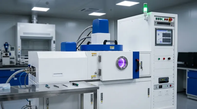
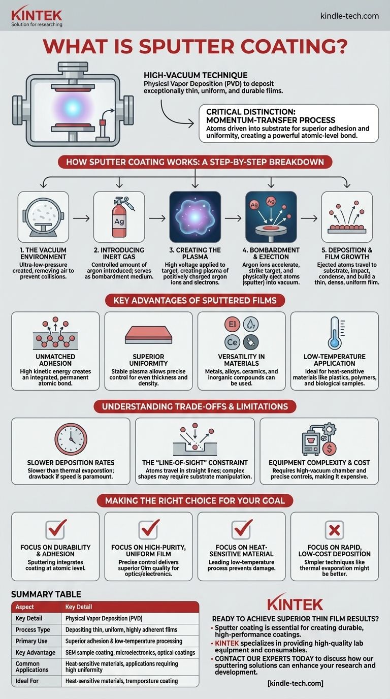
At its core, sputter coating is a high-vacuum technique used to deposit exceptionally thin, uniform, and durable films of material onto a surface. It is a type of Physical Vapor Deposition (PVD) where high-energy ions, typically from an inert gas like argon, bombard a source material (called a "target"). This impact physically ejects, or "sputters," atoms from the target, which then travel through the vacuum and coat the desired object, known as the substrate.
The critical distinction of sputter coating is that it is not merely applying a layer onto a surface. It is a momentum-transfer process that drives atoms into the substrate, creating a powerful, atom-level bond that results in superior adhesion and uniformity compared to many other coating methods.
How Sputter Coating Works: A Step-by-Step Breakdown
To truly understand sputtering, it is best to visualize it as a controlled, atomic-scale sandblasting process where the "sand" is a gas and the ejected particles form a new surface.
The Vacuum Environment
First, the substrate and the target material are placed inside a sealed vacuum chamber. All air is pumped out to create an ultra-low-pressure environment. This step is crucial to prevent the sputtered atoms from colliding with air molecules, which would disrupt the coating process.
Introducing the Inert Gas
A small, precisely controlled amount of an inert gas, most commonly argon, is introduced into the chamber. This gas does not react chemically with the materials but serves as the medium for bombardment.
Creating the Plasma
A high voltage is applied to the target material. This electrical energy strips electrons from the argon gas atoms, creating a glowing, ionized gas known as a plasma. This plasma consists of positively charged argon ions and free electrons.
Bombardment and Ejection
The positively charged argon ions are powerfully accelerated toward the negatively charged target. They collide with the target's surface with significant force, transferring their momentum. This energy transfer is strong enough to knock individual atoms or molecules loose from the target, ejecting them into the vacuum chamber.
Deposition and Film Growth
These ejected target atoms travel in a straight line until they strike the substrate. Upon impact, they condense and build up, layer by layer, to form a thin, dense, and highly uniform film across the substrate's surface.
The Key Advantages of Sputtered Films
The unique mechanism of sputtering provides several distinct benefits that make it the preferred method for many high-performance applications.
Unmatched Adhesion at the Atomic Level
Because the sputtered atoms have high kinetic energy, they don't just land on the substrate—they are driven into its surface. This creates an exceptionally strong, integrated bond. The resulting film becomes a permanent part of the substrate rather than a simple topical coating.
Superior Uniformity and Control
The stable plasma generated during sputtering allows for very fine control over the deposition process. This results in films with excellent uniformity in thickness and density across the entire surface, which is critical for optical and electronic applications.
Versatility in Materials
Sputtering is not limited to metals. A wide range of materials, including alloys, ceramics, and other inorganic compounds, can be used as the target. This allows for the creation of coatings with specific properties like electrical conductivity, wear resistance, or optical reflectivity.
Low-Temperature Application
The sputtering process itself does not generate significant heat on the substrate. This makes it an ideal method for coating heat-sensitive materials such as plastics, polymers, and biological samples for analysis in a Scanning Electron Microscope (SEM).
Understanding the Trade-offs and Limitations
No single process is perfect for every scenario. To make an informed decision, you must be aware of the trade-offs inherent in sputtering.
Slower Deposition Rates
Generally, sputtering is a slower process compared to other PVD techniques like thermal evaporation. For applications where coating thickness is more important than film quality and speed is paramount, this can be a significant drawback.
The 'Line-of-Sight' Constraint
Sputtered atoms travel in a straight line from the target to the substrate. While gas scattering can help coat complex shapes, deeply recessed areas or the backside of an object may not receive a uniform coating without sophisticated substrate rotation and manipulation.
Equipment Complexity and Cost
Sputtering systems require a high-vacuum chamber, precise gas flow controllers, and high-voltage power supplies. This makes the equipment more complex and generally more expensive than simpler coating methods.
Making the Right Choice for Your Goal
Your choice of coating technology should always be driven by the final properties your component requires.
- If your primary focus is durability and adhesion: Sputtering is an excellent choice because it integrates the coating into the substrate at an atomic level.
- If your primary focus is a high-purity, uniform film for optics or electronics: The precise control offered by sputtering delivers superior film quality.
- If your primary focus is coating a heat-sensitive material: Sputtering is a leading low-temperature process that prevents damage to delicate substrates.
- If your primary focus is rapid, low-cost deposition of a simple metal film: You should evaluate whether a simpler technique like thermal evaporation might meet your needs.
Understanding these fundamental principles empowers you to select the right tool for your specific engineering challenge.
Summary Table:
| Aspect | Key Detail |
|---|---|
| Process Type | Physical Vapor Deposition (PVD) |
| Primary Use | Depositing thin, uniform, and highly adherent films |
| Key Advantage | Superior adhesion and low-temperature processing |
| Common Applications | SEM sample coating, microelectronics, optical coatings |
| Ideal For | Heat-sensitive materials, applications requiring high uniformity |
Ready to achieve superior thin film results?
Sputter coating is essential for creating durable, high-performance coatings for electronics, optics, and SEM sample preparation. KINTEK specializes in providing high-quality lab equipment and consumables to meet your specific coating challenges.
Contact our experts today to discuss how our sputtering solutions can enhance your research and development.
Visual Guide
Related Products
- Infrared Transmission Coating Sapphire Sheet Substrate Window
- Electron Beam Evaporation Coating Oxygen-Free Copper Crucible and Evaporation Boat
- 400-700nm Wavelength Anti Reflective AR Coating Glass
- Custom CVD Diamond Coating for Lab Applications
- Molybdenum Tungsten Tantalum Special Shape Evaporation Boat
People Also Ask
- What is optical coating used for? Control Light for Enhanced Performance in Your Applications
- How can we create a reducing environment? Master the Methods for Precise Chemical Control
- Why do we need optical coating? To Control Light and Enhance Optical Performance
- What is the thinnest coating? Unlocking Unique Properties at the Atomic Scale
- Is Sputter Tint good? Premium Heat Rejection & Long-Term Durability Explained


