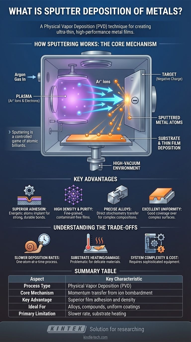
In essence, sputter deposition is a physical vapor deposition (PVD) technique used to create ultra-thin metal films with exceptional control and adhesion. The process works by bombarding a solid metal source, known as the "target," with high-energy ions from a plasma. This atomic-scale collision physically ejects or "sputters" atoms from the target, which then travel through a vacuum and deposit onto a substrate, forming the desired film.
Sputtering is best understood as a highly controlled game of atomic billiards. By using energetic ions to chip away at a metal source atom-by-atom, it builds superior thin films that are denser, more uniform, and adhere more strongly than those made by simpler methods like thermal evaporation.
How Sputtering Works: The Core Mechanism
Sputter deposition is a precise, momentum-driven process that takes place inside a vacuum chamber. Understanding the key steps clarifies why it is so effective for high-performance applications.
The Vacuum Environment
First, the entire process occurs in a high-vacuum chamber. Removing air and other gases is critical to prevent contamination and ensure the sputtered metal atoms have a clear, unobstructed path from the target to the substrate.
Creating the Plasma
An inert gas, most commonly argon, is introduced into the chamber at low pressure. A strong electric field is then applied, which strips electrons from the argon atoms, creating a plasma—an energized soup of positive argon ions (Ar+) and free electrons.
The Target Bombardment
The metal source material, or target, is given a negative electrical charge. This causes the positively charged argon ions from the plasma to accelerate aggressively toward the target, striking its surface with significant kinetic energy.
Atomic Ejection and Deposition
This high-energy bombardment is a pure momentum transfer event. When an argon ion hits the target, it physically knocks out or "sputters" one or more atoms of the target material. These ejected metal atoms travel through the vacuum chamber and land on the substrate, building up the thin film layer by layer.
Key Advantages of Sputter Deposition
Engineers and scientists choose sputtering over other methods when the quality and properties of the thin film are paramount. The benefits stem directly from its energetic, momentum-driven nature.
Superior Film Adhesion
Because sputtered atoms arrive at the substrate with much higher energy than evaporated atoms, they implant slightly into the surface before coming to rest. This creates a strong, durable bond between the film and the substrate that is difficult to achieve with other methods.
High Density and Purity
The energetic deposition process helps form films that are dense and have a fine-grained microstructure. The high vacuum and use of an inert sputtering gas ensure the resulting film has extremely high purity, free from the oxides and contaminants that can plague other techniques.
Control Over Complex Materials
Sputtering is exceptionally good at depositing alloys. The process transfers the stoichiometry (the elemental ratio) of the alloy target directly to the substrate, allowing for the creation of complex metal alloy films with precise compositions. It can also be used to deposit compounds by introducing a reactive gas (like nitrogen or oxygen) into the chamber, a process known as reactive sputtering.
Excellent Step Coverage and Uniformity
While not its strongest point compared to chemical methods, sputtering generally provides better coverage over complex, non-flat surfaces ("step coverage") than simple evaporation. It is also highly effective at producing films of uniform thickness over large areas, which is critical for manufacturing semiconductors and optical coatings.
Understanding the Trade-offs
No technique is perfect. While powerful, sputtering has inherent limitations that make it unsuitable for certain applications.
Slower Deposition Rates
The one-atom-at-a-time nature of sputtering is precise but also relatively slow compared to thermal evaporation. For applications where a thick coating is needed quickly and film quality is less critical, sputtering can be inefficient.
Potential for Substrate Damage and Heating
The high energy of the bombarding ions and depositing atoms can transfer significant heat to the substrate. This can be problematic for delicate substrates like plastics or certain biological samples, potentially causing damage or altering their properties.
System Complexity and Cost
Sputtering systems are more complex and expensive than simple thermal evaporators. They require high-vacuum pumps, sophisticated power supplies (DC or RF), and precise gas flow control, which increases both the initial investment and operational overhead.
Making the Right Choice for Your Goal
Selecting the right deposition method depends entirely on the required properties of your final film.
- If your primary focus is durability and adhesion: Sputtering is the superior choice for creating robust, wear-resistant coatings or foundational layers for subsequent processing.
- If your primary focus is creating a precise metal alloy film: Sputtering offers unmatched control over stoichiometry, ensuring your deposited film has the same composition as your target.
- If your primary focus is coating a heat-sensitive substrate: You must carefully consider sputtering parameters or explore lower-energy alternatives like thermal evaporation.
- If your primary focus is speed and low cost for a simple metal coating: Thermal evaporation is often a more practical and economical solution.
Ultimately, sputtering is the industry standard when the performance, purity, and precision of a thin metal film are non-negotiable.
Summary Table:
| Aspect | Key Characteristic |
|---|---|
| Process Type | Physical Vapor Deposition (PVD) |
| Core Mechanism | Momentum transfer from ion bombardment |
| Key Advantage | Superior film adhesion and density |
| Ideal For | Alloys, compounds, and uniform coatings |
| Primary Limitation | Slower deposition rate and substrate heating |
Ready to enhance your lab's capabilities with precision thin films?
KINTEK specializes in providing high-performance sputter deposition equipment and consumables for laboratories requiring superior film quality, adhesion, and control. Whether you are working on semiconductor fabrication, advanced optics, or durable protective coatings, our solutions are designed to meet your exacting standards.
Contact our experts today to discuss how our sputtering systems can help you achieve your research and production goals.
Visual Guide
Related Products
- Chemical Vapor Deposition CVD Equipment System Chamber Slide PECVD Tube Furnace with Liquid Gasifier PECVD Machine
- HFCVD Machine System Equipment for Drawing Die Nano-Diamond Coating
- RF PECVD System Radio Frequency Plasma-Enhanced Chemical Vapor Deposition RF PECVD
- 915MHz MPCVD Diamond Machine Microwave Plasma Chemical Vapor Deposition System Reactor
- Customer Made Versatile CVD Tube Furnace Chemical Vapor Deposition Chamber System Equipment
People Also Ask
- What happens during deposition chemistry? Building Thin Films from Gaseous Precursors
- How are carbon nanotubes grown? Master Scalable Production with Chemical Vapor Deposition
- What types of substrates are used in CVD to facilitate graphene films? Optimize Graphene Growth with the Right Catalyst
- How expensive is chemical vapor deposition? Understanding the True Cost of High-Performance Coating
- What are the processes of vapor phase deposition? Understand CVD vs. PVD for Superior Thin Films


