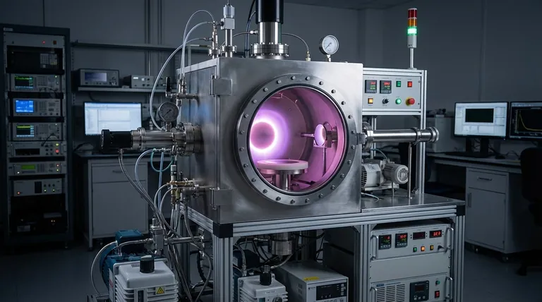
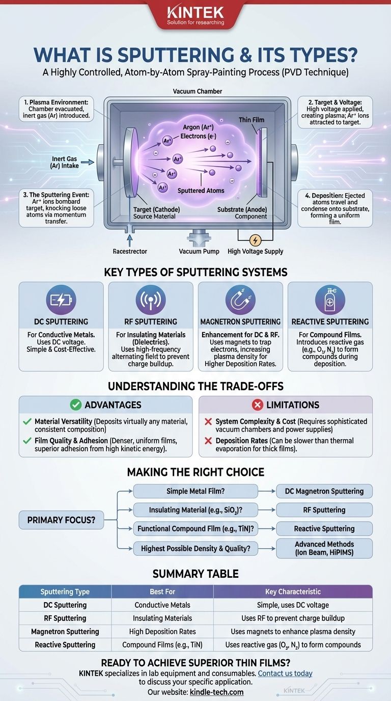
At its core, sputtering is a highly controlled, atom-by-atom spray-painting process. It is a physical vapor deposition (PVD) technique where a source material, called a target, is bombarded by energetic ions from a plasma inside a vacuum chamber. This collision physically ejects, or "sputters," atoms from the target, which then travel and deposit onto a component, known as the substrate, to form an exceptionally thin and uniform film.
The crucial insight is that sputtering is a momentum-transfer process, not an evaporation process. This distinction is what makes it uniquely versatile, enabling the deposition of virtually any material—from pure metals to complex insulators—onto almost any substrate at relatively low temperatures.
The Core Mechanism: From Plasma to Film
Sputtering relies on a sequence of physical events that must be precisely controlled. The entire process takes place within a high-vacuum chamber to ensure the purity of the final film.
Creating the Plasma Environment
First, the chamber is evacuated to remove contaminants. Then, it is backfilled with a small amount of an inert gas, most commonly Argon (Ar). This gas provides the atoms that will be ionized to create the plasma.
The Role of the Target and Voltage
A high voltage is applied to the target, which is the material we want to deposit. This voltage causes the inert gas to break down into a plasma, a glowing state of matter containing positive ions (Ar+) and free electrons. The negatively charged target (cathode) strongly attracts these positively charged Argon ions.
The "Sputtering" Event
Accelerated by the electric field, the Argon ions collide with the target surface with significant force. This impact transfers momentum to the target's atoms, knocking them loose from the surface. These ejected atoms are the "sputtered" material.
Deposition onto the Substrate
The ejected target atoms travel in a straight line through the low-pressure environment until they strike the substrate. Upon impact, they condense and build up, layer by layer, to form a dense and well-adhered thin film.
Key Types of Sputtering Systems
While the physical principle remains the same, the method used to generate and sustain the plasma defines the primary types of sputtering. Each is suited for different materials and applications.
DC Sputtering
Direct Current (DC) sputtering is the simplest form, using a DC voltage to energize the plasma. Because it requires the target to be electrically conductive to maintain the circuit, its use is almost exclusively limited to depositing metals and other conductive materials.
RF Sputtering
Radio Frequency (RF) sputtering uses a high-frequency alternating field instead of a steady DC voltage. The rapid switching of polarity prevents a net charge from building up on the target's surface. This makes RF sputtering essential for depositing insulating (dielectric) and semiconducting materials, such as ceramics or oxides.
Magnetron Sputtering
This is not a standalone type but a critical enhancement that can be applied to both DC and RF systems. Magnetron sputtering uses powerful magnets placed behind the target. These magnets trap electrons near the target surface, dramatically increasing the ionization efficiency of the Argon gas. This results in a denser plasma, leading to significantly higher deposition rates and allowing the process to run at lower pressures.
Reactive Sputtering
Reactive sputtering is a process variation where a reactive gas, such as oxygen or nitrogen, is intentionally introduced into the chamber along with the inert gas. The sputtered metal atoms react with this gas to form a compound film on the substrate. For example, sputtering a titanium target in a nitrogen environment creates a hard, gold-colored Titanium Nitride (TiN) coating.
Understanding the Trade-offs
Sputtering is a powerful technology, but it's essential to understand its advantages and limitations compared to other deposition methods.
Advantage: Material Versatility
Because it is a physical and not a thermal process, sputtering can deposit virtually any material, including complex alloys and compounds. Unlike evaporation, the material's composition remains consistent from the target to the film.
Advantage: Film Quality and Adhesion
Sputtered atoms arrive at the substrate with high kinetic energy. This results in films that are typically much denser, more uniform, and have superior adhesion compared to those from thermal evaporation.
Limitation: System Complexity and Cost
Sputtering systems require sophisticated vacuum chambers, high-voltage power supplies, and potentially complex gas handling. This makes the initial equipment investment higher than for some simpler coating methods.
Limitation: Deposition Rates
While magnetron enhancement significantly improves speed, sputtering can still be slower than high-rate thermal evaporation for depositing thick films of certain pure metals.
Making the Right Choice for Your Goal
Selecting the correct sputtering method is critical for achieving the desired film properties efficiently.
- If your primary focus is depositing a simple metal film: DC Magnetron Sputtering is the most common, fastest, and cost-effective choice.
- If your primary focus is depositing an insulating material like a ceramic (e.g., SiO₂): RF Sputtering is the only viable option to prevent charge buildup and sustain the process.
- If your primary focus is creating a hard, functional compound film (e.g., TiN): Reactive Sputtering is the required method to form the compound during deposition.
- If your primary focus is achieving the highest possible film density and quality: Advanced methods like Ion Beam Sputtering or High-Power Impulse Magnetron Sputtering (HiPIMS) offer unparalleled control.
Ultimately, understanding these fundamental types allows you to select the precise sputtering technique to achieve a high-quality, functional thin film for nearly any application.
Summary Table:
| Sputtering Type | Best For | Key Characteristic |
|---|---|---|
| DC Sputtering | Conductive Metals | Simple, uses DC voltage |
| RF Sputtering | Insulating Materials | Uses radio frequency to prevent charge buildup |
| Magnetron Sputtering | High Deposition Rates | Uses magnets to enhance plasma density |
| Reactive Sputtering | Compound Films (e.g., TiN) | Uses reactive gas (O2, N2) to form compounds |
Ready to Achieve Superior Thin Films?
Choosing the right sputtering method is critical for your research or production success. KINTEK specializes in lab equipment and consumables, providing the precise sputtering solutions you need for depositing metals, ceramics, and complex compounds.
Let our experts help you select the ideal system to ensure high-quality, uniform films with excellent adhesion. Contact us today to discuss your specific application and discover how KINTEK can enhance your laboratory's capabilities.
Visual Guide
Related Products
- Spark Plasma Sintering Furnace SPS Furnace
- Vacuum Induction Melting Spinning System Arc Melting Furnace
- Chemical Vapor Deposition CVD Equipment System Chamber Slide PECVD Tube Furnace with Liquid Gasifier PECVD Machine
- Customer Made Versatile CVD Tube Furnace Chemical Vapor Deposition Chamber System Equipment
People Also Ask
- What is the theory of spark plasma sintering? A Guide to Rapid, Low-Temperature Densification
- What are the fundamentals of spark plasma sintering process? Unlock Rapid, High-Performance Material Consolidation
- What is the pressure for spark plasma sintering? A Guide to Optimizing SPS Parameters
- What technical advantages does a Spark Plasma Sintering (SPS) furnace offer for LZP ceramics? Enhance Ionic Conductivity
- What is the difference between spark plasma sintering and flash sintering? A Guide to Advanced Sintering Methods


