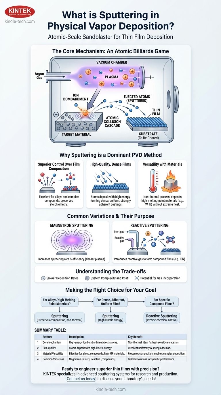
In short, sputtering is a physical vapor deposition (PVD) technique where high-energy ions, typically from an inert gas like argon, are used to bombard a source material, called a target. This collision acts like an atomic-scale sandblaster, knocking atoms off the target. These ejected atoms then travel through a vacuum chamber and deposit onto a substrate, building up a thin, uniform film.
The core principle of sputtering is its non-thermal nature. Instead of melting or boiling a material, it uses pure kinetic energy transfer—an atomic collision cascade—to eject atoms from a solid target, making it exceptionally versatile for depositing a wide range of materials.
The Core Mechanism: An Atomic Billiards Game
To understand sputtering, it's helpful to visualize a game of billiards on an atomic scale. The process relies on a few key components working together within a high-vacuum environment.
The Key Players: Target, Substrate, and Ions
The process involves three main elements. The target is a solid piece of the material you want to deposit. The substrate is the object you want to coat. The ions are the projectiles, created from a process gas (like argon) and accelerated to high energies.
Creating the Plasma
To generate the energetic ions, a low-pressure gas is introduced into the vacuum chamber and energized, often with a strong electric field. This strips electrons from the gas atoms, creating a plasma—an ionized gas containing positively charged ions and free electrons.
The Bombardment Process
A high negative voltage is applied to the target material. The positively charged ions from the plasma are strongly attracted to and accelerate towards this negatively charged target, striking its surface with significant force.
Ejection and Deposition
When an ion hits the target, it transfers its momentum and kinetic energy to the target's atoms. This collision sets off a chain reaction, or collision cascade, that results in surface atoms gaining enough energy to be ejected, or "sputtered," from the target. These vaporized atoms then travel and condense on the substrate, forming the desired thin film.
Why Sputtering is a Dominant PVD Method
Sputtering isn't just one option among many; its unique characteristics make it the preferred choice for many high-performance applications.
Superior Control Over Film Composition
Because sputtering physically knocks atoms from the target, it is excellent for depositing alloys or complex compounds. Unlike thermal evaporation, which can cause materials with different boiling points to separate, sputtering preserves the original composition of the target in the final film.
High-Quality, Dense Films
The sputtered atoms are ejected with significantly higher kinetic energy than atoms from thermal evaporation. This energy helps them form a denser, more uniform, and more strongly adherent film on the substrate, which is critical for durable coatings.
Versatility with Materials
The non-thermal nature of the process means it can deposit materials with extremely high melting points, such as tungsten or titanium, without needing to heat them to extreme temperatures. This opens the door to a vast range of material possibilities.
Common Variations and Their Purpose
The basic sputtering process has been enhanced to improve efficiency and capability for specific applications.
Magnetron Sputtering
This is the most common form of sputtering today. A powerful magnetic field is placed behind the target, which traps electrons from the plasma close to the target's surface. This intensifies the ionization of the gas, creating a denser plasma, which dramatically increases the rate of sputtering and the efficiency of the deposition process.
Reactive Sputtering
In this variation, a reactive gas like nitrogen or oxygen is intentionally introduced into the chamber along with the inert gas. The sputtered metal atoms react with this gas on their way to the substrate, forming a compound film. For example, sputtering a titanium target in a nitrogen atmosphere creates an extremely hard coating of titanium nitride (TiN).
Understanding the Trade-offs
While powerful, sputtering is not without its limitations. Objectivity requires acknowledging where other methods may be more suitable.
Slower Deposition Rates
For some materials, sputtering can be a slower process compared to high-rate thermal evaporation. This can be a factor in high-volume, low-cost production environments.
System Complexity and Cost
Sputtering systems, especially magnetron systems, require sophisticated high-voltage power supplies, magnetic assemblies, and robust vacuum equipment. This can make the initial investment more significant than simpler PVD methods.
Potential for Gas Incorporation
Because the process relies on an inert gas like argon, there is a small risk that some argon atoms can become embedded within the growing film. While often negligible, this can alter the film's electrical or optical properties in sensitive applications.
Making the Right Choice for Your Goal
Selecting the right deposition method depends entirely on the desired properties of the final film.
- If your primary focus is depositing alloys or high-melting-point materials: Sputtering is the superior choice because it avoids thermal decomposition and preserves the target's stoichiometry.
- If your primary focus is achieving a dense, highly adherent, and uniform film: The high kinetic energy of sputtered atoms provides a significant advantage for producing robust, high-performance coatings.
- If your primary focus is creating specific compound films like nitrides or oxides: Reactive sputtering offers precise control over the film's chemical composition and material properties.
Ultimately, sputtering provides an unparalleled level of control and precision for engineering thin films at the atomic level.
Summary Table:
| Feature | Description | Key Benefit |
|---|---|---|
| Core Mechanism | High-energy ions bombard a target, ejecting atoms via momentum transfer. | Non-thermal process; ideal for heat-sensitive materials. |
| Film Quality | Atoms deposit with high kinetic energy, forming dense, adherent films. | Excellent uniformity and strong adhesion to substrates. |
| Material Versatility | Effective for alloys, compounds, and high-melting-point materials (e.g., tungsten). | Preserves target composition; enables complex material deposition. |
| Common Variations | Magnetron sputtering (faster rates) and reactive sputtering (for compound films like TiN). | Tailored solutions for specific performance requirements. |
Ready to engineer superior thin films with precision?
KINTEK specializes in advanced lab equipment and consumables for physical vapor deposition, including sputtering systems tailored to your research or production needs. Whether you're depositing alloys, high-melting-point materials, or custom compounds, our solutions deliver the control and reliability required for high-performance coatings.
Contact us today to discuss how our sputtering expertise can enhance your laboratory's capabilities!
Visual Guide
Related Products
- Spark Plasma Sintering Furnace SPS Furnace
- Vacuum Induction Melting Spinning System Arc Melting Furnace
- Chemical Vapor Deposition CVD Equipment System Chamber Slide PECVD Tube Furnace with Liquid Gasifier PECVD Machine
- Customer Made Versatile CVD Tube Furnace Chemical Vapor Deposition Chamber System Equipment
People Also Ask
- What technical advantages does a Spark Plasma Sintering (SPS) furnace offer for LZP ceramics? Enhance Ionic Conductivity
- What is SPS sintering method? A Guide to High-Speed, High-Performance Material Fabrication
- What is the process fundamentals of spark plasma sintering? Achieve Rapid, High-Density Material Consolidation
- What are the advantages of CAMI/SPS for W-Cu composite preparation? Reduce cycles from hours to seconds.
- What is the theory of spark plasma sintering? A Guide to Rapid, Low-Temperature Densification


