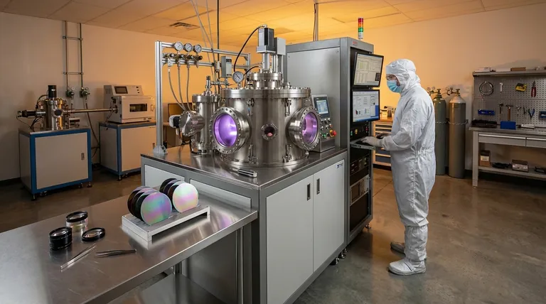
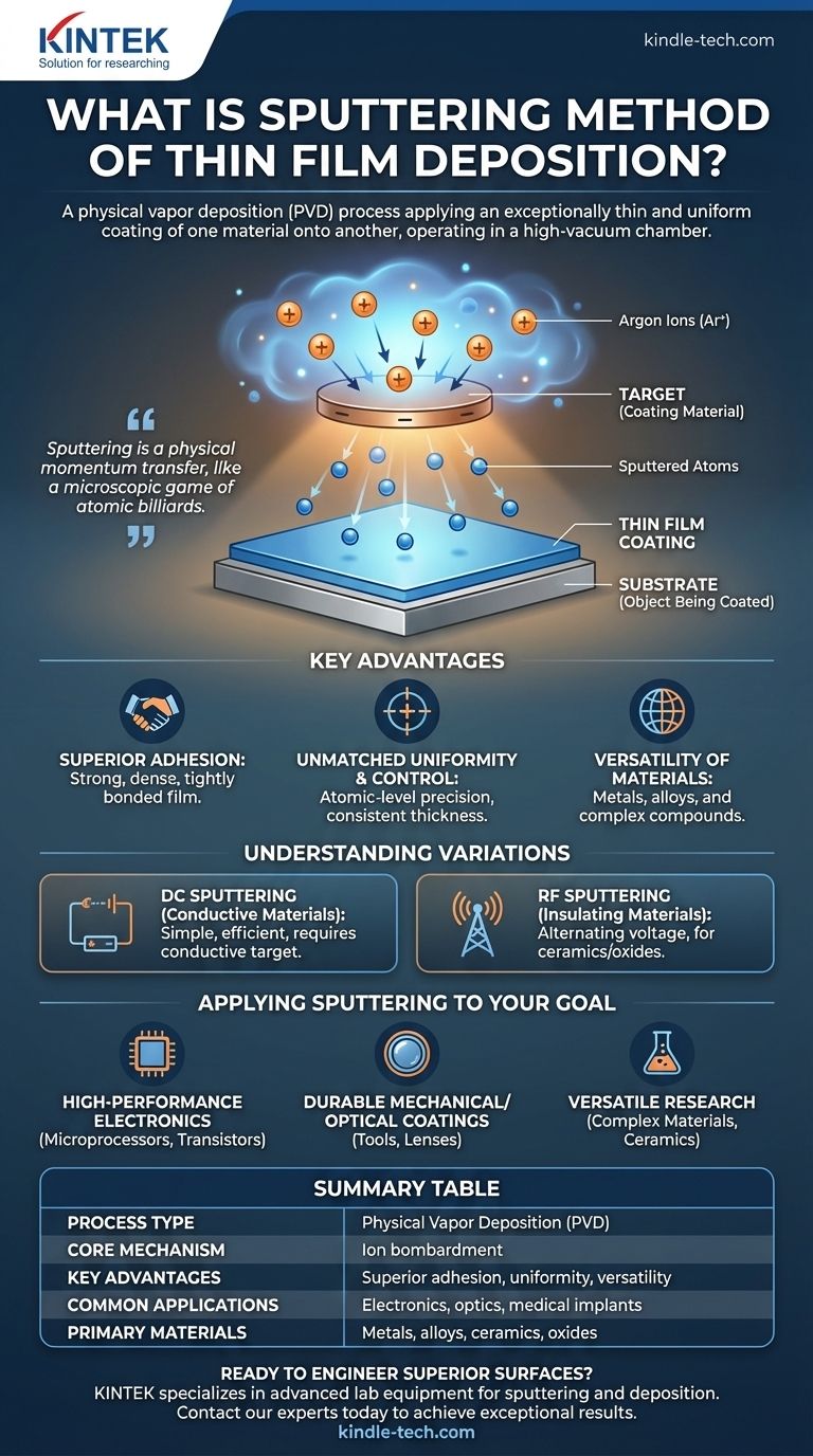
In short, sputtering is a physical deposition process used to apply an exceptionally thin and uniform coating of one material onto another. It operates within a vacuum by creating a plasma and using the resulting ions to bombard a source material, physically knocking atoms loose and depositing them onto a target substrate. This method is a cornerstone of modern manufacturing for components like microprocessors, optical lenses, and medical implants.
Sputtering is not a chemical reaction but a physical momentum transfer, like a microscopic game of atomic billiards. This fundamental difference makes it a highly controllable and versatile technique for precisely engineering the surface properties of nearly any material.
How Sputtering Works: A Physical Process
Sputtering is a type of Physical Vapor Deposition (PVD), meaning the coating material transitions from a solid to a vapor phase and back to a solid, without chemical changes. The entire process takes place in a high-vacuum chamber.
The Core Mechanism: Ion Bombardment
First, the chamber is pumped down to a very low pressure, and a small amount of an inert gas, typically Argon, is introduced.
A high voltage is then applied, which ionizes the Argon gas and creates a glowing plasma. These positively charged Argon ions are accelerated toward a negatively charged plate known as the "target," which is made of the desired coating material.
From Target to Substrate
Upon impact, the high-energy ions physically knock atoms loose from the surface of the target material. This is the "sputtering" effect.
These dislodged atoms travel through the vacuum chamber and land on the "substrate"—the object being coated, such as a silicon wafer or a lens.
The Result: A Uniform Thin Film
Because the sputtered atoms deposit line-of-sight at low pressure, they create a highly uniform and dense coating across the substrate's surface.
This process results in a thin film, often less than a micron thick, with excellent adhesion and precisely controlled thickness.
Why Choose Sputtering? Key Advantages
The physical nature of sputtering provides distinct advantages that make it essential for high-performance applications.
Superior Film Adhesion
The sputtered atoms arrive at the substrate with significant kinetic energy. This energy helps them form a strong, dense, and tightly bonded film that adheres securely to the surface.
Unmatched Uniformity and Control
Sputtering allows for atomic-level control over the deposition process. This results in films with exceptionally consistent thickness and composition, which is critical for optical and semiconductor devices.
Versatility of Materials
This technique can be used to deposit a vast range of materials, including pure metals, alloys, and even complex compounds. This flexibility is a major advantage over other deposition methods that rely on evaporation.
Understanding the Trade-offs and Variations
While powerful, sputtering is not a one-size-fits-all solution. The specific technique must be matched to the material being deposited.
DC Sputtering: For Conductive Materials
The simplest form is Direct Current (DC) sputtering. It is highly efficient but requires the target material to be electrically conductive to maintain the plasma-generating electrical circuit.
RF Sputtering: For Insulating Materials
For non-conductive (dielectric) materials like ceramics or oxides, Radio Frequency (RF) sputtering is used. It alternates the voltage at high frequency, preventing charge from building up on the target and allowing the plasma to be sustained.
Common Pitfalls to Avoid
The primary trade-offs for sputtering are its relatively slow deposition rate compared to thermal evaporation and its requirement for complex high-vacuum systems. Incorrect pressure or power settings can lead to poor film quality or damage to the substrate.
Applying Sputtering to Your Goal
Choosing the right approach depends entirely on the desired outcome for your component's surface.
- If your primary focus is high-performance electronics: Sputtering offers the precision and uniformity required to deposit the conductive and dielectric layers in microprocessors and transistors.
- If your primary focus is durable mechanical or optical coatings: The excellent adhesion and density of sputtered films create hard, wear-resistant, and anti-reflective surfaces for tools and lenses.
- If your primary focus is versatile research with complex materials: RF sputtering provides the capability to work with a wide array of insulating compounds, oxides, and ceramics that other methods cannot handle.
Ultimately, sputtering is a foundational technology that enables the precise modification of a material's surface to achieve entirely new levels of performance.
Summary Table:
| Feature | Description |
|---|---|
| Process Type | Physical Vapor Deposition (PVD) |
| Core Mechanism | Ion bombardment of a target material |
| Key Advantages | Superior adhesion, unmatched uniformity, material versatility |
| Common Applications | Microprocessors, optical lenses, medical implants, wear-resistant coatings |
| Primary Materials | Metals, alloys, ceramics, oxides (via RF sputtering) |
Ready to engineer superior surfaces with precision thin films? KINTEK specializes in advanced lab equipment and consumables for sputtering and other deposition techniques. Whether you're developing high-performance electronics, durable optical coatings, or researching new materials, our solutions deliver the control and reliability your laboratory needs. Contact our experts today to discuss how we can support your specific application and help you achieve exceptional results.
Visual Guide
Related Products
- Spark Plasma Sintering Furnace SPS Furnace
- Vacuum Induction Melting Spinning System Arc Melting Furnace
- Chemical Vapor Deposition CVD Equipment System Chamber Slide PECVD Tube Furnace with Liquid Gasifier PECVD Machine
- Customer Made Versatile CVD Tube Furnace Chemical Vapor Deposition Chamber System Equipment
People Also Ask
- What technical advantages does a Spark Plasma Sintering (SPS) furnace offer for LZP ceramics? Enhance Ionic Conductivity
- What is SPS sintering method? A Guide to High-Speed, High-Performance Material Fabrication
- What is the mechanism of SPS process? A Deep Dive into Rapid, Low-Temperature Sintering
- Why are Spark Plasma Sintering (SPS) furnaces or hot presses utilized in the preparation of Li3PS4 solid electrolytes?
- What is the pressure for spark plasma sintering? A Guide to Optimizing SPS Parameters


