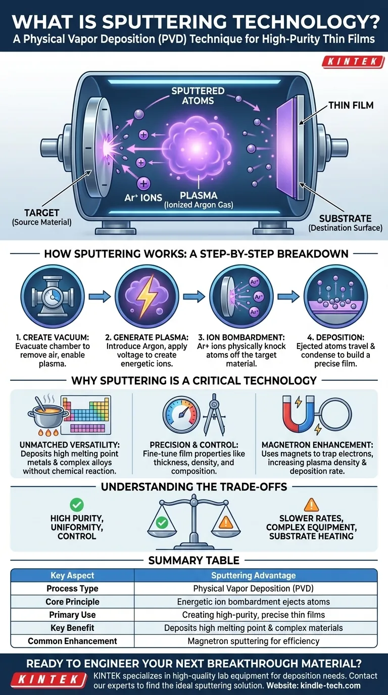
At its core, sputtering is a physical vapor deposition (PVD) technique used to create ultra-thin, highly uniform coatings or films on a surface. The process works by placing a source material (the "target") and a destination surface (the "substrate") in a vacuum chamber. An energized, inert gas like Argon is introduced, and its ions are accelerated to bombard the target, physically knocking off atoms which then travel and deposit onto the substrate.
Creating high-purity, precisely controlled thin films from a wide array of materials is a fundamental challenge in advanced manufacturing. Sputtering addresses this by offering a physical deposition method that provides exceptional control over film properties, regardless of a material's melting point or chemical reactivity.
How Sputtering Works: A Step-by-Step Breakdown
The sputtering process is a carefully orchestrated sequence of physical events occurring at the atomic level inside a vacuum chamber. Each step is critical to achieving a high-quality film.
Step 1: Creating the Vacuum Environment
First, the substrate (such as a silicon wafer or piece of glass) and the target material are placed inside a sealed chamber. This chamber is evacuated to a high vacuum.
This vacuum is crucial for two reasons: it removes atmospheric gases that could contaminate the film, and it provides the low-pressure conditions necessary to generate and sustain a plasma.
Step 2: Generating the Plasma
An inert gas, most commonly Argon (Ar), is introduced into the chamber. A high negative voltage is then applied to the target material.
This strong electric field ionizes the Argon gas, stripping electrons from the Argon atoms and creating a mixture of positively charged Argon ions (Ar+) and free electrons. This energized cloud of ions and electrons is called a plasma.
Step 3: The Bombardment Process
The positively charged Argon ions within the plasma are powerfully attracted to the negatively charged target. They accelerate toward the target at high velocity.
Upon impact, the energetic ions physically collide with the target's surface, transferring their momentum and knocking loose, or "sputtering," individual atoms or small clusters of atoms from the target material.
Step 4: Deposition onto the Substrate
The ejected atoms from the target travel through the low-pressure environment of the chamber. They eventually land on the surface of the substrate.
As these atoms accumulate, they condense and bond to the substrate, gradually building up a thin, solid film. The process allows for precise control over the final film's thickness and uniformity.
Why Sputtering is a Critical Technology
Sputtering isn't just one of many options; it is often the only viable option for creating specific types of advanced materials and devices. Its advantages solve key manufacturing challenges.
Unmatched Material Versatility
Unlike chemical processes (like CVD) or thermal evaporation, sputtering is a physical process that does not rely on melting or chemical reactions.
This makes it exceptionally effective for depositing materials with extremely high melting points (like tungsten or tantalum) and complex alloys whose composition must be preserved precisely in the final film.
Precision and Control
Sputtering provides engineers with fine-grained control over the final film's properties.
By adjusting parameters like gas pressure, power, and substrate temperature, one can precisely dictate the film's density, grain size, morphology, and electrical or optical properties. This level of control is essential for semiconductors, optical filters, and other high-performance components.
The Role of Magnetron Sputtering
A common enhancement to the basic process is magnetron sputtering. This technique uses powerful magnets placed behind the target.
The magnetic field traps electrons in a circular path close to the target's surface. This dramatically increases the probability of electrons colliding with and ionizing Argon atoms, leading to a denser plasma, a more efficient sputtering process, and significantly faster deposition rates.
Understanding the Trade-offs
While powerful, sputtering technology has specific operational considerations and limitations that must be weighed against its benefits.
Slower Deposition Rates
Compared to some high-rate processes like thermal evaporation, sputtering can have a lower deposition rate. This can be a limiting factor in high-volume manufacturing where throughput is paramount. Magnetron sputtering helps mitigate this but does not eliminate the trade-off entirely.
High Vacuum and Equipment Complexity
Sputtering requires a high-quality vacuum to prevent contamination and sustain the plasma. The necessary equipment, including robust vacuum chambers and high-performance pumps, can be complex and represent a significant capital investment.
Potential for Substrate Damage
The bombardment of the substrate by various energetic particles, including the sputtered atoms themselves, can transfer energy and cause heating or even minor structural damage. This can be a concern when coating delicate or heat-sensitive substrates.
Making the Right Choice for Your Goal
Selecting the right deposition technology depends entirely on the specific requirements of your material, substrate, and final application.
- If your primary focus is material flexibility: Sputtering is ideal for depositing refractory metals, ceramics, or complex alloys that are challenging or impossible to deposit using thermal or chemical methods.
- If your primary focus is precise film quality: Choose sputtering when you require exact control over film thickness, density, stoichiometry, and electrical properties for advanced electronic or optical devices.
- If your primary focus is coating complex 3D shapes: While possible, sputtering is a line-of-sight process. Other methods like CVD or atomic layer deposition (ALD) may offer better conformity on highly complex, non-planar geometries.
By understanding its core principles, you can leverage sputtering to engineer materials at the atomic level, enabling the next generation of advanced products.
Summary Table:
| Key Aspect | Sputtering Advantage |
|---|---|
| Process Type | Physical Vapor Deposition (PVD) |
| Core Principle | Energetic ion bombardment to eject target atoms |
| Primary Use | Creating high-purity, precisely controlled thin films |
| Key Benefit | Deposits materials with high melting points and complex alloys |
| Common Enhancement | Magnetron sputtering for higher efficiency and faster rates |
Ready to Engineer Your Next Breakthrough Material?
Sputtering technology is the foundation for creating the high-performance thin films that power modern electronics, optics, and advanced materials. Whether you are developing semiconductors, optical coatings, or specialized surfaces, the right equipment is critical to your success.
KINTEK specializes in high-quality lab equipment and consumables for all your deposition needs. Our expertise can help you select the ideal sputtering solution to achieve precise control over film properties, ensure material purity, and accelerate your R&D or production.
Let's discuss how we can support your laboratory's goals. Contact our experts today to find the perfect sputtering solution for your application.
Visual Guide
Related Products
- Spark Plasma Sintering Furnace SPS Furnace
- Vacuum Induction Melting Spinning System Arc Melting Furnace
- Chemical Vapor Deposition CVD Equipment System Chamber Slide PECVD Tube Furnace with Liquid Gasifier PECVD Machine
- Customer Made Versatile CVD Tube Furnace Chemical Vapor Deposition Chamber System Equipment
People Also Ask
- Why are Spark Plasma Sintering (SPS) furnaces or hot presses utilized in the preparation of Li3PS4 solid electrolytes?
- What is the process fundamentals of spark plasma sintering? Achieve Rapid, High-Density Material Consolidation
- What are the fundamentals of spark plasma sintering process? Unlock Rapid, High-Performance Material Consolidation
- What are the advantages of CAMI/SPS for W-Cu composite preparation? Reduce cycles from hours to seconds.
- What is the pressure for spark plasma sintering? A Guide to Optimizing SPS Parameters


