At its core, the primary advantage of Chemical Vapor Deposition (CVD) over Physical Vapor Deposition (PVD) is its ability to create highly uniform, or conformal, coatings over complex shapes and even inside deep crevices. Because CVD uses a chemical reaction from a gas phase, it is not restricted by the line-of-sight limitations that constrain PVD processes, allowing it to coat surfaces that are not directly exposed to the source material.
The choice between CVD and PVD is not about which is universally "better," but is a critical engineering trade-off. CVD offers superior coverage on complex geometries, while PVD provides a lower-temperature process suitable for more delicate substrates.
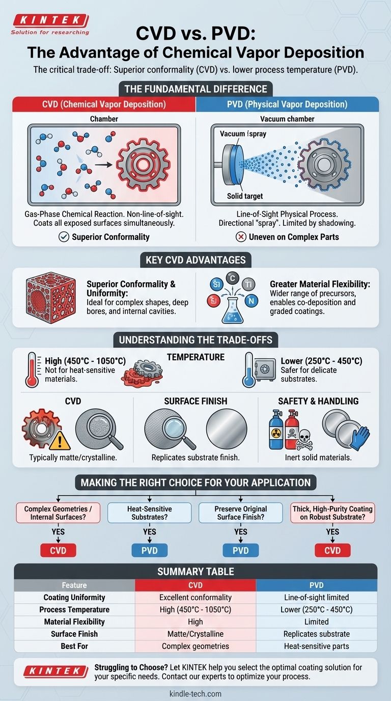
The Fundamental Difference: Chemical vs. Physical
To understand the advantages of each process, you must first understand how they fundamentally differ. The method of deposition dictates the properties of the final coating.
How CVD Works: A Gas-Phase Chemical Reaction
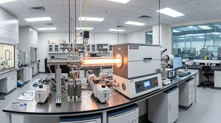
CVD is a chemical process. Gaseous molecules, known as precursors, are introduced into a reaction chamber where they decompose and react with the substrate surface at high temperatures.
This reaction forms a new, solid material layer directly on the substrate. Because the entire component is immersed in the reactive gas, deposition occurs on all exposed surfaces simultaneously.
How PVD Works: A Line-of-Sight Physical Process
PVD is a physical process, essentially a "spray coating" on an atomic level. A solid source material is vaporized into a plasma of atoms or molecules inside a vacuum chamber.
An electrical field then accelerates these particles, causing them to travel in a straight line and impact the substrate, where they condense to form a coating. Any area not in the direct line of sight of the source will not be coated effectively.
Key Advantages of CVD
The chemical, non-directional nature of CVD gives it several distinct advantages in specific scenarios.
Superior Conformality and Uniformity
This is CVD's most significant advantage. Since the deposition is driven by a chemical reaction in a gaseous environment, it is not limited by line-of-sight.
This allows CVD to deposit a uniform coating on parts with intricate geometries, deep bores, sharp corners, and internal cavities. PVD struggles with these applications, often resulting in thin or non-existent coatings in "shadowed" areas.
Greater Material and Compositional Flexibility
CVD can utilize any element that can be sourced as a volatile chemical compound. This opens up a wider range of potential coating materials compared to PVD, which is limited to materials that can be effectively vaporized or sputtered from a solid target.
Furthermore, CVD allows for the co-deposition of different materials by simply mixing precursor gases, enabling the creation of composite or graded coatings with unique properties.
Understanding the Trade-offs
Choosing CVD for its advantages means accepting its inherent trade-offs. In many cases, PVD is the more practical and effective choice.
The Critical Factor of Temperature
CVD is a high-temperature process, typically operating between 450°C and 1050°C. This extreme heat is necessary to drive the chemical reactions.
This temperature range makes CVD unsuitable for many heat-sensitive materials, such as tempered steels, aluminum alloys, or plastics, which would be damaged or distorted. PVD operates at much lower temperatures (typically 250°C to 450°C), making it compatible with a far wider range of substrates.
Surface Finish and Post-Processing
PVD coatings are known for replicating the substrate's original surface finish with high fidelity. A polished part will remain polished after a PVD coating.
CVD, however, typically results in a matte or crystalline finish due to its growth mechanism. Achieving a smooth, polished surface on a CVD-coated part often requires expensive and time-consuming post-processing.
Safety and Material Handling
The precursor gases used in many CVD processes can be toxic, corrosive, or even pyrophoric (igniting spontaneously in air).
This introduces significant safety, storage, and handling challenges that are generally less severe in PVD processes, which primarily work with inert solid materials in a vacuum.
Making the Right Choice for Your Application
The decision must be driven by the specific requirements of your component and its intended function.
- If your primary focus is coating complex geometries or internal surfaces: CVD's non-line-of-sight capability makes it the definitive choice.
- If you are working with heat-sensitive substrates: PVD's lower process temperature is almost always the necessary selection.
- If preserving the original surface finish is critical for function or aesthetics: PVD is the preferred method to avoid post-processing.
- If you require a thick, high-purity coating on a robust substrate that can withstand high heat: CVD can be a highly effective and economical solution.
Ultimately, selecting the correct coating technology requires a clear understanding of your engineering goal and the material limitations involved.
Summary Table:
| Feature | CVD (Chemical Vapor Deposition) | PVD (Physical Vapor Deposition) |
|---|---|---|
| Coating Uniformity | Excellent conformality on complex shapes | Line-of-sight limited, uneven on complex parts |
| Process Temperature | High (450°C - 1050°C) | Lower (250°C - 450°C) |
| Material Flexibility | High (wide range of precursors) | Limited (solid target materials) |
| Surface Finish | Typically matte/crystalline | Replicates substrate finish |
| Best For | Complex geometries, internal surfaces | Heat-sensitive substrates, fine finishes |
Struggling to Choose the Right Coating Technology for Your Components?
At KINTEK, we specialize in helping laboratories and manufacturers select the optimal coating solution for their specific needs. Whether you're working with intricate parts requiring CVD's superior conformality or heat-sensitive materials needing PVD's gentle process, our expertise ensures you get the right equipment and consumables for your application.
Let us help you:
- Optimize your coating process for better performance and efficiency
- Select the right equipment for your specific substrate and geometry requirements
- Access high-quality consumables and ongoing technical support
Contact our coating experts today for a personalized consultation and discover how KINTEK's lab equipment solutions can enhance your research or production outcomes.
Get in touch with our team now →
Visual Guide
Related Products
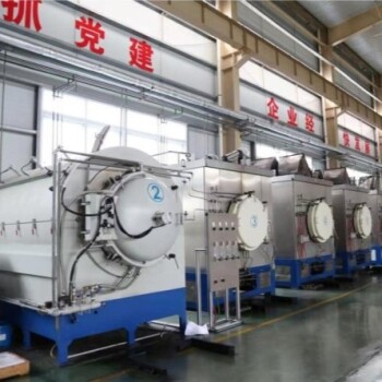
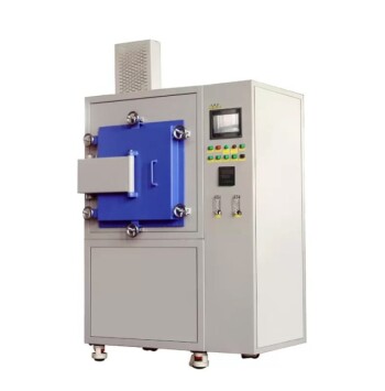
- Chemical Vapor Deposition CVD Equipment System Chamber Slide PECVD Tube Furnace with Liquid Gasifier PECVD Machine
- RF PECVD System Radio Frequency Plasma-Enhanced Chemical Vapor Deposition RF PECVD
- Inclined Rotary Plasma Enhanced Chemical Vapor Deposition PECVD Equipment Tube Furnace Machine
- Customer Made Versatile CVD Tube Furnace Chemical Vapor Deposition Chamber System Equipment
- 1400℃ Laboratory Quartz Tube Furnace with Alumina Tube Tubular Furnace
People Also Ask
- What are the advantages of PECVD over CVD? Achieve High-Quality Thin Films at Lower Temperatures
- How are PECVD and CVD different? A Guide to Choosing the Right Thin-Film Deposition Process
- What is the difference between CVD and PVD process? A Guide to Choosing the Right Coating Method
- What are the examples of CVD method? Discover the Versatile Applications of Chemical Vapor Deposition
- How plasma is generated in PECVD? A Step-by-Step Breakdown of the Process