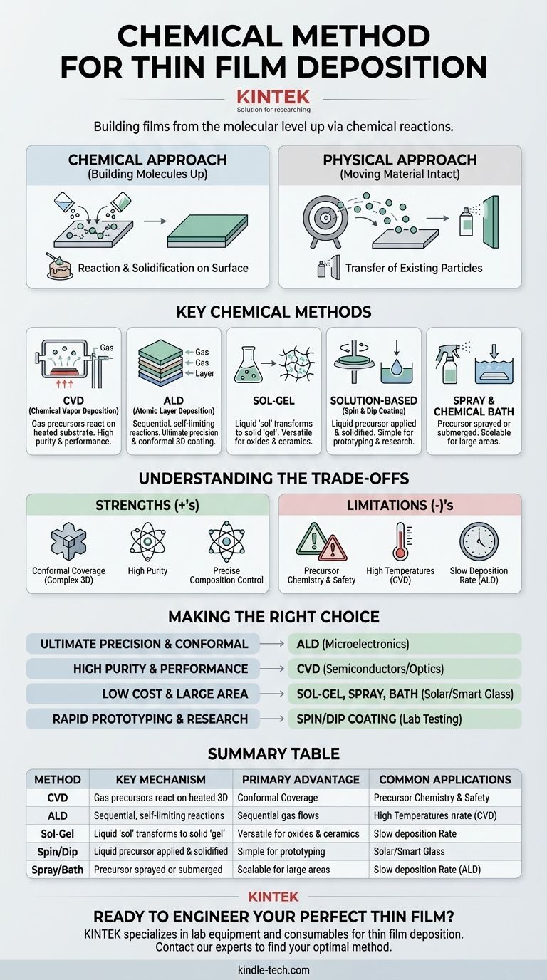
In short, chemical methods for thin film deposition use chemical reactions to create a solid film on a substrate from precursor materials. Unlike physical methods that transfer a solid material, chemical techniques build the film from the molecular level up using processes like Chemical Vapor Deposition (CVD), Atomic Layer Deposition (ALD), sol-gel, and spin coating.
The fundamental difference is one of assembly. Physical deposition is like spray-painting a wall, where existing particles of paint are moved from a can to the surface. Chemical deposition is like frosting a cake, where you mix ingredients (precursors) that react and solidify directly on the surface to form the final layer.
The Two Pillars of Deposition: Chemical vs. Physical
To truly understand chemical deposition, it's essential to contrast it with its counterpart, physical deposition. All thin film creation falls into one of these two categories.
The Chemical Approach: Building from the Molecules Up
Chemical methods rely on the transformation of precursor materials. These precursors, often in a liquid or gas phase, undergo a chemical reaction on or near the substrate surface.
This reaction causes them to convert into the desired solid material, forming a thin, stable film. This bottom-up assembly is the defining characteristic.
The Physical Approach: Moving Material Intact
Physical Vapor Deposition (PVD) methods, such as sputtering or thermal evaporation, work differently. They start with a solid source material (a "target").
High energy, either from heat or plasma, is used to vaporize atoms from the target. These atoms then travel through a vacuum and re-condense on the cooler substrate, forming the film without a fundamental chemical reaction.
A Breakdown of Key Chemical Methods
Several techniques fall under the chemical deposition umbrella, each with unique mechanisms and ideal use cases.
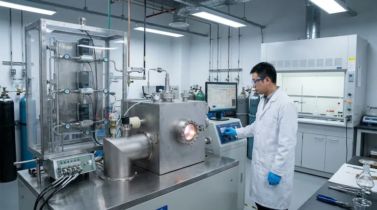
Chemical Vapor Deposition (CVD)
CVD is a workhorse in the semiconductor industry. It involves introducing precursor gases into a reaction chamber containing the substrate.
High temperatures cause these gases to react and decompose on the substrate surface, leaving behind a high-purity, high-performance film. A common variant is Plasma-Enhanced CVD (PECVD), which uses plasma to enable these reactions at lower temperatures.
Atomic Layer Deposition (ALD)
ALD is a specialized subset of CVD that offers the ultimate control over film thickness and uniformity. It builds the film one single atomic layer at a time.
This is achieved by introducing precursor gases sequentially, with each gas completing a self-limiting reaction on the surface. This allows for perfect, "conformal" coatings on even the most complex 3D structures.
Sol-Gel
The sol-gel process begins with a chemical solution, or "sol," containing molecular precursors. This solution is applied to a substrate, often through spin or dip coating.
Through a controlled drying and heating process, the solution undergoes a phase change into a solid gel and finally a dense, solid film. This method is highly versatile for creating oxide and ceramic coatings.
Spin Coating and Dip Coating
These are simple, solution-based techniques for applying a liquid precursor. In spin coating, the substrate is spun at high speed, using centrifugal force to spread the liquid into an extremely thin, uniform layer.
In dip coating, the substrate is slowly submerged in and withdrawn from a chemical bath, leaving a controlled layer of the liquid precursor to solidify.
Spray Pyrolysis & Chemical Bath
Spray pyrolysis involves spraying a precursor solution onto a heated substrate. The heat causes the droplets to undergo a chemical reaction (pyrolysis), depositing a solid film.
The chemical bath method is even more direct. The substrate is simply submerged in a solution where controlled chemical reactions cause the desired material to precipitate and grow on its surface.
Understanding the Trade-offs
Choosing a chemical method involves clear advantages but also requires acknowledging specific limitations.
Strength: Conformal Coverage and Purity
Because gas-phase precursors can reach every nook and cranny of a surface, methods like CVD and especially ALD are unmatched for creating uniform coatings on complex, non-flat objects. The nature of the chemical reactions also tends to produce films with very high chemical purity.
Strength: Precise Control Over Composition
By carefully managing the mixture of precursor materials, you can precisely control the final chemical composition (stoichiometry) of the film. This is critical for advanced materials like compound semiconductors and complex oxides.
Limitation: Precursor Chemistry and Safety
The success of any chemical method depends entirely on the availability of suitable precursor chemicals. These precursors can be expensive, highly toxic, flammable, or difficult to handle, requiring specialized equipment and safety protocols.
Limitation: Temperature and Deposition Rate
Many CVD processes require very high temperatures, which can damage sensitive substrates like polymers. Furthermore, some chemical methods, particularly ALD, are inherently slow due to their layer-by-layer mechanism.
Making the Right Choice for Your Goal
Selecting the correct method depends entirely on your project's priorities, from precision and performance to cost and scale.
- If your primary focus is ultimate precision and conformal coating: ALD is the unmatched choice for its atomic-level control, essential for modern microelectronics.
- If your primary focus is high-purity, high-performance films: CVD and its variants are the industry standard for creating robust films for semiconductors and optics.
- If your primary focus is low-cost, large-area coating: Solution-based methods like sol-gel, spray pyrolysis, or chemical bath offer excellent scalability for applications like smart glass or solar cells.
- If your primary focus is rapid prototyping or research: Spin coating and dip coating provide simple, accessible, and inexpensive ways to test new material formulations in a lab.
By understanding the principles behind each chemical method, you can engineer a film with the exact properties your project demands.
Summary Table:
| Method | Key Mechanism | Primary Advantage | Common Applications |
|---|---|---|---|
| Chemical Vapor Deposition (CVD) | Gas-phase precursors react on a heated substrate. | High-purity, high-performance films. | Semiconductors, optics. |
| Atomic Layer Deposition (ALD) | Sequential, self-limiting surface reactions. | Ultimate precision & conformal coating on complex 3D structures. | Microelectronics, nanotechnology. |
| Sol-Gel | Liquid precursor transforms into a solid network. | Versatility for oxides/ceramics; cost-effective for large areas. | Solar cells, smart glass, protective coatings. |
| Spin Coating / Dip Coating | Liquid precursor spread by spinning or dipping. | Simple, inexpensive, rapid prototyping. | Research, photoresists. |
| Spray Pyrolysis / Chemical Bath | Precursor solution sprayed or substrate submerged. | Scalability for large-area coatings. | Solar cells, sensors. |
Ready to Engineer Your Perfect Thin Film?
The right deposition method is critical to your project's success. Whether you need the atomic-level precision of ALD for advanced R&D or the scalable performance of CVD for production, KINTEK has the expertise and equipment to help.
We specialize in providing lab equipment and consumables for all your thin film deposition needs. Contact our experts today to discuss your specific application and discover the optimal chemical method to achieve the film properties you demand.
Visual Guide
Related Products
- Aluminized Ceramic Evaporation Boat for Thin Film Deposition
- Tungsten Evaporation Boat for Thin Film Deposition
- Electron Beam Evaporation Coating Oxygen-Free Copper Crucible and Evaporation Boat
- Molybdenum Tungsten Tantalum Evaporation Boat for High Temperature Applications
- Vacuum Hot Press Furnace Machine for Lamination and Heating
People Also Ask
- What are the applications of thin films deposition? Unlock New Possibilities for Your Materials
- What are thin films deposited by evaporation? A Guide to High-Purity Coating
- What is the widely used boat made of in thermal evaporation? Choosing the Right Material for High-Purity Deposition
- What is the source of evaporation for thin film? Choosing Between Thermal and E-Beam Methods
- Why is an alumina boat and Ti3AlC2 powder bed necessary for Ti2AlC sintering? Protect MAX Phase Purity


