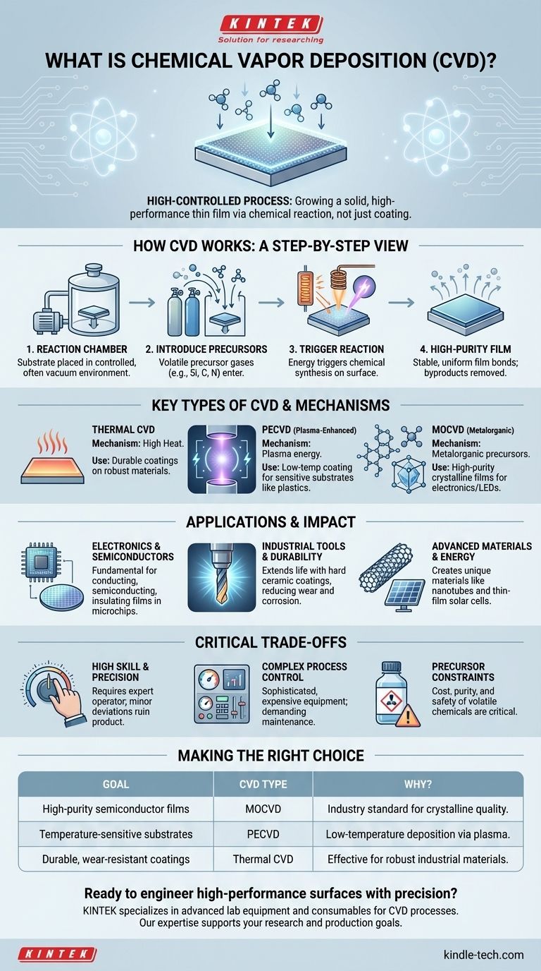
In essence, Chemical Vapor Deposition (CVD) is a highly controlled process used to apply a solid, high-performance thin film onto a surface. It works by introducing reactive gases, known as precursors, into a chamber where they undergo a chemical reaction at the surface of a target object, known as a substrate. This reaction forms a solid layer, effectively "growing" a new material directly onto the substrate's surface.
The core principle of CVD is not merely coating a surface, but initiating a precise chemical reaction that synthesizes a new, high-purity solid material directly onto an object. This distinction is what makes it a foundational process in manufacturing advanced electronics and materials.
How Chemical Vapor Deposition Works: A Step-by-Step View
Understanding CVD requires seeing it as a controlled chemical synthesis rather than a simple application process. The environment and inputs are meticulously managed to achieve the desired outcome.
The Reaction Chamber
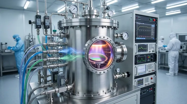
First, the substrate—the part to be coated—is placed inside a sealed reaction chamber. This chamber allows for precise control over the environment, often involving a vacuum to remove contaminants and manage pressure.
Introducing the Precursor Gases
One or more volatile precursor chemicals are introduced into the chamber in gaseous form. These precursors contain the specific atoms required for the final thin film (e.g., silicon, carbon, nitrogen).
Triggering the Chemical Reaction
An energy source is used to trigger the chemical reaction on the substrate's surface. The precursors decompose and react, depositing the desired solid material atom by atom. The specific energy source used defines the type of CVD process.
The Result: A High-Purity Thin Film
The byproduct gases from the reaction are exhausted from the chamber, leaving behind a stable, uniform, and high-purity thin film bonded to the substrate. The thickness and properties of this film can be controlled with extreme precision.
Key Types of CVD and Their Mechanisms
The method used to supply energy and deliver precursors differentiates the various types of CVD, each tailored for specific materials and applications.
Thermal CVD: The Foundation
Thermal CVD is the most fundamental type, using high heat to provide the energy needed for the chemical reaction. The substrate is heated, and when the precursor gases contact the hot surface, they react and deposit the film.
Plasma-Enhanced CVD (PECVD): Lower Temperatures
Plasma-Enhanced CVD (PECVD) uses an electric field to generate a plasma (an ionized gas) within the chamber. This plasma provides the energy for the reaction, allowing the process to occur at much lower temperatures than thermal CVD, which is critical for temperature-sensitive substrates like plastics or certain electronics.
Metalorganic CVD (MOCVD): High-Purity Crystalline Films
This specialized process uses metalorganic compounds as precursors. MOCVD is essential in the electronics industry for growing high-quality crystalline films, such as those used in manufacturing LEDs and high-performance semiconductors.
Other Specialized Delivery Methods
Other variations focus on how the precursor is delivered. Aerosol-assisted CVD (AACVD) uses an aerosol, while Direct Liquid Injection (DLI-CVD) involves injecting a liquid precursor into a heated zone where it vaporizes before reaching the substrate.
Understanding the Applications and Impact
The precision of CVD makes it indispensable across numerous high-tech industries for creating materials with enhanced properties.
In Electronics and Semiconductors
CVD is fundamental to modern electronics. It is used to deposit the various thin films—conducting, semiconducting, and insulating—that form the intricate structures of microchips, processors, and memory devices.
For Industrial Tools and Durability
In manufacturing, CVD applies extremely hard ceramic coatings to cutting tools, drills, and machine parts. These coatings drastically reduce wear and prevent corrosion, significantly extending the life and performance of the equipment.
In Advanced Materials and Energy
The process is used to create materials with unique properties, such as growing carbon nanotubes and nanowires. It is also critical in manufacturing thin-film solar cells by depositing photovoltaic materials onto a substrate like glass or metal.
The Critical Trade-offs of CVD
While powerful, CVD is a complex process that requires significant expertise and investment to execute correctly.
The Need for High Skill and Precision
Achieving a uniform, high-quality film requires an expert operator. Factors like temperature, pressure, gas flow rates, and precursor chemistry must be controlled with extreme precision, as even minor deviations can ruin the final product.
Complexity of Process Control
The equipment for CVD is sophisticated and expensive. Maintaining the vacuum, managing reactive and sometimes hazardous gases, and ensuring consistent energy delivery requires a robust and well-maintained system.
Precursor Material Constraints
The choice of precursor chemicals is critical. They must be volatile enough to be used in a gaseous state but stable enough to be handled safely. The cost, purity, and safety of these precursors are significant considerations in any CVD operation.
Making the Right Choice for Your Goal
Selecting the correct CVD method is entirely dependent on the material of your substrate and the desired properties of the final film.
- If your primary focus is creating highly pure semiconductor films for electronics: MOCVD is specifically designed for this level of crystalline quality and is an industry standard.
- If you are working with temperature-sensitive substrates like polymers: PECVD is the superior choice because its use of plasma allows for deposition at much lower temperatures.
- If you need exceptionally durable, wear-resistant coatings on robust materials: Thermal CVD is a common, effective, and well-understood method for these industrial applications.
Ultimately, mastering Chemical Vapor Deposition provides the power to engineer materials at the atomic level, building high-performance surfaces from the ground up.
Summary Table:
| CVD Type | Key Mechanism | Primary Use Case |
|---|---|---|
| Thermal CVD | Uses high heat to trigger reaction | Durable, wear-resistant coatings on robust materials |
| PECVD | Uses plasma for lower temperature reactions | Coating temperature-sensitive substrates (e.g., plastics) |
| MOCVD | Uses metalorganic precursors | High-purity crystalline films for semiconductors and LEDs |
Ready to engineer high-performance surfaces with precision?
The controlled synthesis of thin films is critical for innovation in your lab. KINTEK specializes in providing the advanced lab equipment and consumables needed for processes like Chemical Vapor Deposition. Whether you are developing next-generation semiconductors, durable industrial coatings, or advanced materials, our expertise supports your research and production goals.
Contact us today to discuss how our solutions can enhance your capabilities and help you achieve superior results. [#ContactForm]
Visual Guide
Related Products
- Chemical Vapor Deposition CVD Equipment System Chamber Slide PECVD Tube Furnace with Liquid Gasifier PECVD Machine
- Customer Made Versatile CVD Tube Furnace Chemical Vapor Deposition Chamber System Equipment
- HFCVD Machine System Equipment for Drawing Die Nano-Diamond Coating
- Split Chamber CVD Tube Furnace with Vacuum Station Chemical Vapor Deposition System Equipment Machine
- Multi Heating Zones CVD Tube Furnace Machine Chemical Vapor Deposition Chamber System Equipment
People Also Ask
- How expensive is chemical vapor deposition? Understanding the True Cost of High-Performance Coating
- What is the chemical vapor deposition growth process? Build Superior Thin Films from the Atom Up
- What types of substrates are used in CVD to facilitate graphene films? Optimize Graphene Growth with the Right Catalyst
- What is plasma enhanced chemical vapor deposition PECVD equipment? A Guide to Low-Temperature Thin Film Deposition
- What are the core advantages of PE-CVD in OLED encapsulation? Protect Sensitive Layers with Low-Temp Film Deposition


