In nanotechnology, Chemical Vapor Deposition (CVD) is a "bottom-up" fabrication technique used to grow high-purity, ultra-thin solid films onto a surface. It works by introducing reactive gases (precursors) into a chamber where they undergo a chemical reaction on a heated substrate, depositing a new layer of material atom by atom. This method is foundational for creating nanostructures and advanced materials like graphene and semiconductor films with precise control over their thickness and properties.
CVD is not merely a coating technology; it is a controlled chemical construction process at the atomic scale. Its core value lies in its ability to build uniform, chemically bonded materials on a substrate, making it an indispensable tool for fabricating the high-performance components central to modern nanotechnology.

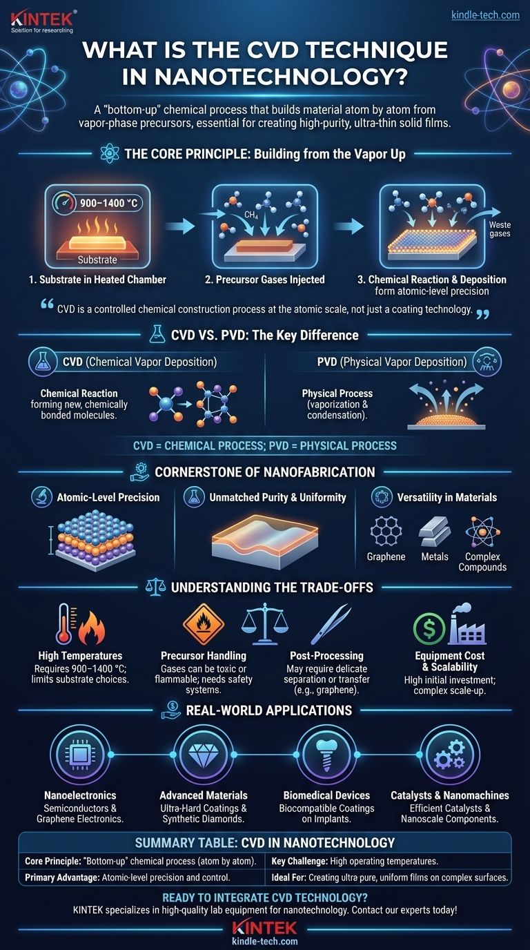
The Core Principle: Building from the Vapor Up
CVD is a process of synthesis. Unlike methods that carve material away, CVD builds new material directly onto a surface through a controlled chemical reaction.
The Reaction Chamber Setup
The process begins with a substrate—the object to be coated—placed inside a vacuum chamber. This chamber is heated to a specific, often very high, temperature.
The Role of Precursor Gases
One or more volatile precursor gases are then injected into the chamber. These gases contain the chemical elements required to form the final film. For example, to create graphene (a form of carbon), a carbon-bearing gas like methane is used.
The Deposition Reaction
When the hot precursor gases come into contact with the heated substrate, a chemical reaction is triggered. This reaction breaks down the precursor molecules and causes a solid material to deposit onto the substrate, forming a thin, stable film. Often, the substrate itself is coated with a catalyst (like copper for graphene) to facilitate this reaction.
The Key Difference: CVD vs. PVD
It's crucial to distinguish CVD from Physical Vapor Deposition (PVD). PVD is a physical process, like evaporation or sputtering, where a material is vaporized and then simply condenses onto a substrate. CVD is a chemical process where new molecules are formed and deposited, resulting in a chemically bonded, often crystalline or amorphous, film.
Why CVD is a Cornerstone of Nanofabrication
CVD's properties make it uniquely suited for the demands of nanotechnology, where performance is dictated by features measured in single atoms.
Atomic-Level Precision
The primary advantage of CVD is its control. By carefully managing temperature, pressure, and gas flow, engineers can control the film's growth rate and thickness with atomic-level precision. This is essential for creating materials like single-layer graphene or complex semiconductor stacks.
Unmatched Purity and Uniformity
Because the process starts with highly pure gases in a controlled environment, the resulting films are exceptionally pure. The nature of the vapor transport allows the film to grow uniformly across the entire substrate, even on complex, non-flat surfaces.
Versatility in Materials and Structures
CVD is not limited to one type of material. It can be used to create simple monoatomic films, metals, complex multi-component compounds, and intermetallic oxides. Specialized variants like Metalorganic CVD (MOCVD) are used to grow intricate crystalline layers for high-performance electronics.
Understanding the Trade-offs of CVD
While powerful, CVD is not a universal solution. Its effectiveness depends on balancing its strengths against its operational requirements.
The Challenge of High Temperatures
Standard CVD processes often operate at very high temperatures, typically between 900–1400 °C. This heat can damage or destroy many types of substrates, limiting its application to materials that can withstand such extreme conditions.
Precursor Handling and Safety
The gases used in CVD can be toxic, corrosive, or flammable. This necessitates sophisticated handling systems, safety protocols, and exhaust management, which adds to the operational complexity and cost.
Potential for Post-Processing
In many applications, the work isn't finished after deposition. For instance, graphene grown on a copper catalyst must be carefully separated from the metal and transferred to its final target substrate, which is a delicate and complex process.
Equipment Cost and Scalability
While described as "cost-effective" for large-scale production, the initial investment in high-quality CVD reactors, vacuum pumps, and gas handling systems is significant. Achieving process control for large-area deposition requires substantial engineering effort.
Real-World Applications in Nanotechnology
CVD is the enabling technology behind many breakthroughs in science and industry.
Nanoelectronics and Semiconductors
CVD is the backbone of the semiconductor industry, used to deposit the critical thin films that make up microprocessors and memory chips. It is also the primary method for producing large-area graphene for next-generation flexible electronics and transparent conductors.
Advanced Materials and Coatings
The technique is used to create some of the world's most durable materials. This includes synthetic diamonds, ultra-hard coatings for cutting tools, and corrosion-resistant layers that protect components in harsh environments.
Biomedical Devices
CVD is used to apply biocompatible and durable coatings onto medical implants. These coatings can improve an implant's integration with the body and prevent degradation over time.
Catalysts and Nanomachines
By depositing specific materials onto nanostructured scaffolds, CVD can create highly efficient catalysts. It is also used to fabricate components for nanoscale machines and sensors.
Making the Right Choice for Your Goal
Selecting a fabrication method requires aligning the technique's capabilities with your specific objective.
- If your primary focus is creating ultra-pure, single-layer materials like graphene: CVD is the industry-standard method due to its unparalleled control over atomic layer growth.
- If your primary focus is coating complex, three-dimensional nanostructures: CVD's ability to deposit a uniform film over contoured surfaces makes it superior to line-of-sight methods like PVD.
- If your primary focus is mass production of semiconductor films: Specialized, large-scale CVD systems are essential for achieving the required purity and uniformity across large wafers.
- If your primary focus is working with heat-sensitive substrates: You must investigate lower-temperature CVD variants (like Plasma-Enhanced CVD) or choose an entirely different deposition method.
Ultimately, understanding CVD is to understand how to harness controlled chemical reactions to build functional materials from the atom up.
Summary Table:
| Key Aspect | CVD in Nanotechnology |
|---|---|
| Core Principle | A "bottom-up" chemical process that builds material atom by atom from vapor-phase precursors. |
| Primary Advantage | Atomic-level precision and control over film thickness and properties. |
| Key Challenge | Often requires very high temperatures, which can limit substrate choices. |
| Ideal For | Creating ultra-pure, uniform films on complex surfaces (e.g., graphene, semiconductor layers). |
Ready to integrate CVD technology into your research or production line? KINTEK specializes in providing high-quality lab equipment and consumables for nanotechnology applications. Our expertise can help you select the right tools to achieve precise, high-purity material deposition for your projects in semiconductors, advanced materials, and beyond. Contact our experts today to discuss your specific laboratory needs and discover how we can support your innovation.
Visual Guide
Related Products
- CVD Diamond Dressing Tools for Precision Applications
- Multi Heating Zones CVD Tube Furnace Machine Chemical Vapor Deposition Chamber System Equipment
- CVD Diamond Domes for Industrial and Scientific Applications
- CVD Diamond for Thermal Management Applications
- Chemical Vapor Deposition CVD Equipment System Chamber Slide PECVD Tube Furnace with Liquid Gasifier PECVD Machine
People Also Ask
- How do you identify a CVD diamond? The Definitive Guide to Lab-Grown Diamond Verification
- How long does it take to make synthetic diamonds? Discover the 6-8 Week Science Behind Lab-Grown Gems
- What are the raw materials for CVD diamonds? A seed, a gas, and the science of crystal growth.
- What color diamonds are CVD? Understanding the Process from Brown Tint to Colorless Beauty
- Can CVD diamonds change color? No, their color is permanent and stable.


