In materials science and manufacturing, sputtering is a physical vapor deposition (PVD) method used to create exceptionally thin and uniform material layers, or "thin films." The process works by bombarding a source material, known as a target, with high-energy ions inside a vacuum chamber. This bombardment acts like a microscopic sandblasting, ejecting atoms from the target, which then travel and deposit onto a substrate to form a dense, high-purity film.
Sputtering is fundamentally a physical momentum-transfer process, not a chemical one. This distinction is critical, as it allows for the deposition of a wide range of materials—including pure metals, alloys, and compounds—with precise control over the final film's thickness and composition.
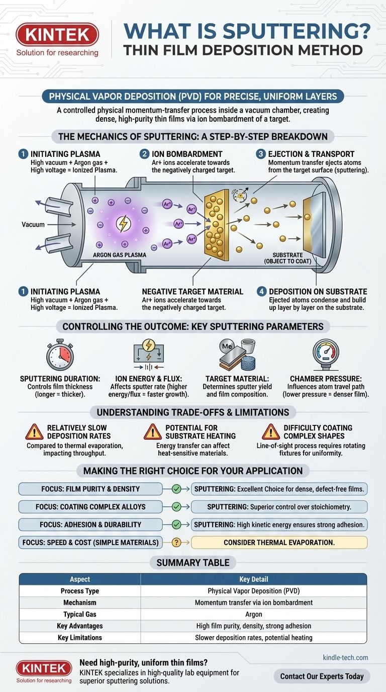
The Mechanics of Sputtering: A Step-by-Step Breakdown
To truly understand sputtering, it's helpful to visualize it as a controlled, atomic-level sequence of events occurring within a vacuum chamber.
Initiating the Plasma
First, the chamber is pumped down to a high vacuum to remove contaminants. An inert gas, typically Argon, is then introduced at a very low pressure. A high voltage is applied, which strips electrons from the Argon atoms, creating a glowing, ionized gas known as a plasma.
Ion Bombardment of the Target
The source material to be deposited is shaped into a "target" and given a strong negative electrical charge. The positively charged Argon ions from the plasma are accelerated by the electric field and crash into the negatively charged target at high speed.
Ejection and Transport
Each collision transfers kinetic energy from the Argon ion to the target. If enough energy is transferred, it will knock out, or "sputter," atoms from the target material. These ejected atoms travel in a straight line through the low-pressure environment.
Deposition onto the Substrate
The ejected target atoms eventually strike all surfaces within the chamber, including the object to be coated, which is called the substrate. Upon hitting the substrate, the atoms condense and build up, layer by layer, to form a solid, uniform thin film. These films are often only a few hundred nanometers thick.
Controlling the Outcome: Key Sputtering Parameters
The quality and characteristics of the sputtered film are not left to chance. They are precisely controlled by manipulating several key process parameters.
Sputtering Duration
The most straightforward control is time. The thickness of the deposited film is directly proportional to the duration of the sputtering process. Longer deposition times result in thicker films.
Ion Energy and Flux
The energy of the bombarding ions, which can range from tens to thousands of electron volts, dictates how effectively they eject atoms from the target. Higher energy and a higher number of ions (ion flux) increase the sputter rate, leading to faster film growth.
Target Material
Different materials have different sputter yields. This means that for a given ion bombardment, some materials will eject atoms more readily than others. The choice of target material is fundamental to the process.
Chamber Pressure
The pressure of the inert gas inside the chamber affects how the sputtered atoms travel. Lower pressure allows for a more direct "line-of-sight" path to the substrate, often resulting in a denser film.
Understanding the Trade-offs of Sputtering
While powerful, sputtering is not a universal solution. Understanding its limitations is crucial for making informed engineering decisions.
Relatively Slow Deposition Rates
Compared to thermal evaporation, where material is essentially boiled off, sputtering is often a slower process. This can impact throughput in high-volume manufacturing environments.
Potential for Substrate Heating
The high-energy ion bombardment is not perfectly efficient. A significant amount of energy is transferred to the substrate as heat. This can be a major issue when coating heat-sensitive materials like plastics or certain optical components.
Difficulty Coating Complex Shapes
Because sputtering is largely a line-of-sight process, achieving a uniform coating on complex, three-dimensional objects can be challenging. It often requires sophisticated rotating fixtures to ensure all surfaces are adequately exposed to the flow of sputtered atoms.
Making the Right Choice for Your Application
Use these guidelines to determine if sputtering aligns with your project's primary goal.
- If your primary focus is film purity and density: Sputtering is an excellent choice because it physically transfers the target material with high fidelity, creating dense and defect-free films.
- If your primary focus is coating complex alloys or compounds: Sputtering offers superior control over stoichiometry (the elemental ratio) because it ejects all elements from a composite target at a predictable rate.
- If your primary focus is adhesion and durability: The high kinetic energy of sputtered atoms helps them implant slightly into the substrate surface, leading to exceptionally strong film adhesion.
- If your primary focus is speed and cost for a simple material: You may want to evaluate thermal evaporation, which can offer higher deposition rates for certain pure metals.
By understanding these core mechanics and trade-offs, you can confidently leverage sputtering to engineer thin films with precise and repeatable properties.
Summary Table:
| Sputtering Aspect | Key Detail |
|---|---|
| Process Type | Physical Vapor Deposition (PVD) |
| Mechanism | Momentum transfer via ion bombardment |
| Typical Gas | Argon |
| Key Advantages | High film purity, density, and strong adhesion |
| Key Limitations | Slower deposition rates, potential substrate heating |
Need a high-purity, uniform thin film for your lab?
Sputtering is a powerful technique for creating precise coatings, but choosing the right equipment is critical for your results. KINTEK specializes in high-quality lab equipment and consumables, including sputtering systems, to help you achieve superior film deposition with excellent adhesion and stoichiometric control.
Contact our experts today to discuss your specific laboratory needs and discover how our solutions can enhance your research and development.
Visual Guide
Related Products
- Spark Plasma Sintering Furnace SPS Furnace
- Vacuum Induction Melting Spinning System Arc Melting Furnace
- Chemical Vapor Deposition CVD Equipment System Chamber Slide PECVD Tube Furnace with Liquid Gasifier PECVD Machine
- Customer Made Versatile CVD Tube Furnace Chemical Vapor Deposition Chamber System Equipment
People Also Ask
- What are the advantages of CAMI/SPS for W-Cu composite preparation? Reduce cycles from hours to seconds.
- What is the pressure for spark plasma sintering? A Guide to Optimizing SPS Parameters
- What is the process fundamentals of spark plasma sintering? Achieve Rapid, High-Density Material Consolidation
- What is the theory of spark plasma sintering? A Guide to Rapid, Low-Temperature Densification
- What is the mechanism of SPS process? A Deep Dive into Rapid, Low-Temperature Sintering


