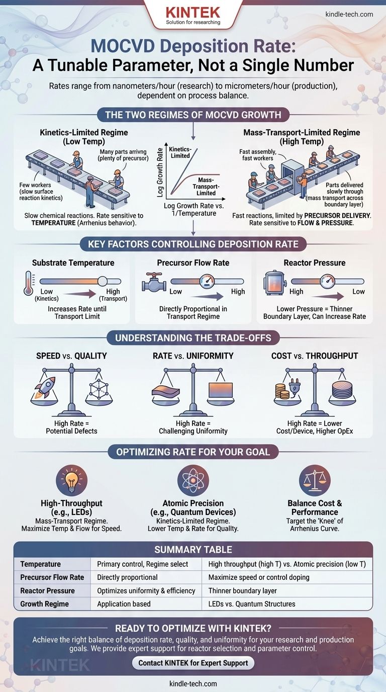
In short, the deposition rate for Metal-Organic Chemical Vapor Deposition (MOCVD) is not a single number but a highly tunable parameter. While typical rates for industrial applications like LED manufacturing can range from 1 to 10 micrometers (μm) per hour, rates for research or atomically precise structures can be deliberately slowed to just a few nanometers per hour. The specific rate is a direct result of the process conditions you choose.
The central challenge of MOCVD is not simply achieving a high deposition rate, but rather understanding and controlling the balance between two competing physical processes: the mass transport of precursor gases to the wafer and the surface reaction kinetics that govern how atoms incorporate into the crystal. Mastering this balance is the key to optimizing for speed, quality, or cost.
The Two Regimes of MOCVD Growth
The deposition rate in an MOCVD reactor is fundamentally governed by a "rate-limiting step"—the slowest part of the overall process. This creates two distinct operational regimes, primarily determined by the substrate temperature.
The Mass-Transport-Limited Regime
At higher temperatures, the chemical reactions on the substrate surface are extremely fast. The growth is therefore limited by how quickly the precursor gas molecules can be transported from the main gas flow, across a stagnant boundary layer, to the wafer surface.
Think of it as an assembly line where the workers are incredibly fast. The overall production speed is limited only by how quickly you can deliver parts to them. In this regime, the growth rate is relatively insensitive to small changes in temperature but highly dependent on precursor flow rates and reactor pressure.
The Reaction-Kinetics-Limited Regime
At lower temperatures, the opposite is true. There are plenty of precursor molecules available at the surface, but the chemical reactions needed to break them down and incorporate atoms into the crystal lattice are slow.
This is an assembly line with a surplus of parts, but the workers themselves are slow. The production speed is determined by their personal efficiency. In this regime, the growth rate is extremely sensitive to temperature, following a predictable exponential relationship (Arrhenius behavior), but less sensitive to the precursor flow rate.
Visualizing the Regimes
This relationship is often visualized in a classic Arrhenius plot, which shows the logarithm of the growth rate versus the inverse of the temperature (1/T). The plot reveals a flat "plateau" at high temperatures (mass-transport limited) and a steep, linear decline at low temperatures (kinetics-limited). Most industrial processes operate in the mass-transport-limited regime for stability and high throughput.
Key Factors Controlling Deposition Rate
To control the deposition rate, an engineer or scientist manipulates a few critical parameters.
Substrate Temperature
Temperature is the primary lever for selecting your growth regime. Increasing temperature pushes the process from being kinetics-limited to mass-transport-limited, generally increasing the deposition rate until the transport limit is reached.
Precursor Flow Rate
The concentration of the metal-organic precursors in the carrier gas is a direct control knob. In the mass-transport-limited regime, doubling the precursor flow rate will roughly double the deposition rate, assuming the reactor can maintain stable flow dynamics.
Reactor Pressure
Total pressure inside the reaction chamber affects the gas flow velocity and the thickness of the boundary layer above the wafer. Lowering the pressure can thin this boundary layer, improving the efficiency of mass transport and thus increasing the deposition rate.
Carrier Gas Flow and Type
The inert carrier gas (typically hydrogen or nitrogen) that transports the precursors also plays a role. Higher total gas flows can reduce the residence time of precursors in the reactor and alter the boundary layer, subtly influencing the final growth rate and uniformity.
Understanding the Trade-offs
Simply maximizing the deposition rate is rarely the ultimate goal. The pursuit of speed comes with critical trade-offs that impact the final device quality and cost.
Speed vs. Quality
This is the most fundamental trade-off. High deposition rates can increase the likelihood of incorporating defects into the crystal lattice, leading to lower material quality. For applications requiring atomically smooth interfaces and low defect density, such as quantum wells or high-electron-mobility transistors (HEMTs), a slower, more controlled growth in the kinetics-limited regime is essential.
Rate vs. Uniformity
Achieving a high growth rate that is perfectly uniform across a large-diameter wafer is a major engineering challenge. High gas flows can create turbulence and temperature gradients, causing the film to be thicker in some areas and thinner in others. Optimizing reactor geometry and gas injection is critical to managing this.
Cost vs. Throughput
A higher deposition rate directly translates to higher wafer throughput, which lowers the manufacturing cost per device. However, this often requires running the reactor at higher temperatures and using higher precursor flow rates, which increases precursor consumption (a major cost driver) and energy usage.
Optimizing Rate for Your Specific Goal
The "best" deposition rate is entirely dependent on your objective. Use these principles as a guide for setting up your MOCVD process.
- If your primary focus is high-throughput production (e.g., LEDs): Operate firmly in the mass-transport-limited regime by using high temperatures and maximizing precursor flow rates for the fastest stable growth.
- If your primary focus is atomically precise layers (e.g., quantum heterostructures): Operate in the kinetics-limited regime with lower temperatures and slower rates to achieve monolayer control and superior material quality.
- If your primary focus is balancing cost and performance: Target the "knee" of the Arrhenius curve—the transition point between the two regimes—to achieve a respectable growth rate without a significant penalty in material quality.
Ultimately, mastering MOCVD deposition rate is about consciously choosing your operating conditions to achieve a predictable and repeatable outcome for your specific material and device goals.
Summary Table:
| Parameter | Effect on Deposition Rate | Typical Goal |
|---|---|---|
| Temperature | Primary control; increases rate until mass-transport limit | High throughput (high temp) vs. atomic precision (low temp) |
| Precursor Flow Rate | Directly proportional in mass-transport regime | Maximize speed or control doping/stoichiometry |
| Reactor Pressure | Lower pressure thins boundary layer, can increase rate | Optimize for uniformity and efficiency |
| Growth Regime | Mass-transport-limited (fast, stable) vs. Kinetics-limited (slow, precise) | Choose based on application: LEDs vs. quantum structures |
Ready to Optimize Your MOCVD Process?
Whether you are scaling up production for LED manufacturing or developing next-generation quantum devices, achieving the right balance of deposition rate, film quality, and uniformity is critical. KINTEK specializes in providing the lab equipment and expert support to meet your specific thin-film research and production goals.
We help you:
- Select the right reactor configuration for your target growth regime.
- Precisely control process parameters like temperature and precursor flow for reproducible results.
- Achieve superior material quality and wafer-scale uniformity.
Let's discuss your project. Our team is ready to help you master your MOCVD process.
Contact KINTEK today to speak with an expert
Visual Guide
Related Products
- Multi Heating Zones CVD Tube Furnace Machine Chemical Vapor Deposition Chamber System Equipment
- 915MHz MPCVD Diamond Machine Microwave Plasma Chemical Vapor Deposition System Reactor
- Microwave Plasma Chemical Vapor Deposition MPCVD Machine System Reactor for Lab and Diamond Growth
- Cylindrical Resonator MPCVD Machine System Reactor for Microwave Plasma Chemical Vapor Deposition and Lab Diamond Growth
- Molybdenum Vacuum Heat Treat Furnace
People Also Ask
- What is the function of a tube furnace in CVD SiC synthesis? Achieving Ultra-Pure Silicon Carbide Powders
- How does a CVD tube furnace inhibit the sintering of silver supports? Boost Membrane Durability and Performance
- What are the advantages of using a Multi-zone Tube Furnace? Enhanced Thermal Uniformity for Diffusion Research
- What advantages do CVD furnaces offer for Wf/W composites? Preserving Fiber Ductility and Interface Integrity
- What is the function of a high-temperature CVD tube furnace in 3D graphene foam prep? Master 3D Nanomaterial Growth