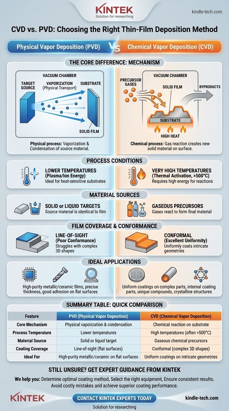
At its core, the difference between Chemical Vapor Deposition (CVD) and Physical Vapor Deposition (PVD) lies in how the coating material transitions from its source to the target surface. PVD physically transports the material by vaporizing a solid or liquid source and condensing it onto the substrate. In contrast, CVD uses reactive precursor gases that undergo a chemical reaction directly on the substrate's surface to create a new, solid material as a thin film.
The fundamental distinction is one of mechanism: PVD is a physical process of vaporization and condensation, while CVD is a chemical process where gases react to form a solid film. This single difference dictates their respective process conditions, capabilities, and ideal applications.
The Core Mechanism: Physical vs. Chemical Transformation
To truly understand these technologies, you must first grasp their fundamentally different approaches to building a thin film. One is a process of physical transport, while the other is a process of chemical creation.
Physical Vapor Deposition (PVD): A "Source-to-Target" Journey
PVD is a line-of-sight process. It begins with a solid material, often called a "target," inside a vacuum chamber.
This solid source is then vaporized into atoms or molecules using physical means. This can be done by heating it until it evaporates or by bombarding it with high-energy ions, a process known as sputtering.
These vaporized particles travel directly through the vacuum and physically condense onto the cooler substrate, forming the desired thin film. The material of the film is the same as the material of the source; it has only undergone a change of state (solid → vapor → solid).
Chemical Vapor Deposition (CVD): Creating a Film from Gaseous Precursors
CVD is a chemical reaction process. It does not start with the final coating material in solid form.
Instead, one or more volatile gases, known as precursor gases, are introduced into a reaction chamber containing the heated substrate.
When these gases come into contact with the hot surface, they react or decompose, leaving behind a solid film of a new material. The excess gas and byproducts are then pumped out of the chamber.
Key Process Characteristics
The difference in mechanism leads to distinct process requirements and outcomes for the resulting film.
The Role of Temperature
CVD processes traditionally require very high temperatures (often several hundred to over a thousand degrees Celsius) to provide the necessary activation energy for the chemical reactions to occur on the substrate surface.
PVD can often be performed at lower temperatures, as it relies on physical energy sources (like plasma or electron beams) rather than thermal energy alone. This makes PVD suitable for coating materials that cannot withstand high heat.
Material Sources
The starting materials are completely different. PVD uses a solid or liquid source of the exact material you wish to deposit.
CVD relies on gaseous chemical precursors, which contain the elements needed to form the final film through a reaction.
Film Coverage and Conformance
Because PVD is a line-of-sight technique, it excels at coating flat surfaces. However, it struggles to uniformly coat complex, three-dimensional shapes, as "shadowed" areas will receive little to no coating.
CVD, by contrast, uses gases that can flow around and into intricate features. This allows it to produce highly conformal coatings that uniformly cover even the most complex geometries.
Understanding the Trade-offs
Neither method is universally superior; the choice depends entirely on the application's specific requirements.
PVD: Precision and Material Variety
PVD offers excellent control over film thickness and can be used to deposit a vast range of materials, including metals, alloys, and certain ceramics with very high melting points. It is prized for its ability to create dense, hard, and high-purity films with strong adhesion.
CVD: Conformal Coatings and Unique Materials
CVD is the champion of uniformity and conformal coverage. It is the go-to method for coating the inside of complex parts or creating uniform layers in semiconductor manufacturing. The chemical process also allows for the formation of unique compounds and crystalline structures that may be difficult to achieve with PVD.
Common Pitfalls to Avoid
A common mistake is choosing a method based on familiarity rather than requirements. Using PVD on a complex part can lead to non-uniform, unreliable coatings. Conversely, using high-temperature CVD on a temperature-sensitive substrate can damage or destroy the part.
Making the Right Choice for Your Application
Your final decision must be driven by the specific goal you need to achieve for your component or device.
- If your primary focus is coating a complex, 3D shape uniformly: CVD is almost always the correct choice due to its superior conformal coverage.
- If your primary focus is depositing a high-purity metallic or ceramic film on a relatively flat surface: PVD offers excellent control, a wide material selection, and typically good adhesion.
- If your primary focus is coating a temperature-sensitive substrate: PVD or a specialized variant like Plasma-Assisted CVD (PACVD) are your necessary options.
Understanding the fundamental difference between physical transport and chemical reaction is the key to selecting the right technology for your specific engineering challenge.
Summary Table:
| Feature | PVD (Physical Vapor Deposition) | CVD (Chemical Vapor Deposition) |
|---|---|---|
| Core Mechanism | Physical vaporization & condensation | Chemical reaction on substrate surface |
| Process Temperature | Lower temperatures | High temperatures (often >500°C) |
| Material Source | Solid or liquid target | Gaseous chemical precursors |
| Coating Coverage | Line-of-sight (good for flat surfaces) | Conformal (excellent for complex 3D shapes) |
| Ideal For | High-purity metallic/ceramic films on flat surfaces | Uniform coatings on intricate geometries |
Still Unsure Which Coating Method is Right for Your Application?
Choosing between PVD and CVD can be complex, but you don't have to make this critical decision alone. KINTEK specializes in laboratory equipment and consumables, serving researchers and engineers who require precise thin-film deposition solutions.
We can help you:
- Determine the optimal coating method for your specific substrate and performance requirements
- Select the right equipment for your laboratory's unique needs
- Ensure your thin-film processes deliver consistent, reliable results
Our expertise in lab equipment means we understand the nuances of both PVD and CVD technologies. Let us help you avoid costly mistakes and achieve superior coating performance.
Contact our experts today for a personalized consultation and discover how KINTEK can enhance your laboratory's capabilities.
Visual Guide
Related Products
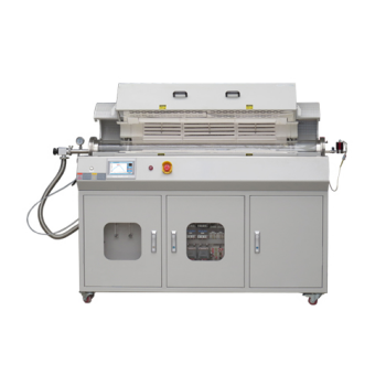
- Chemical Vapor Deposition CVD Equipment System Chamber Slide PECVD Tube Furnace with Liquid Gasifier PECVD Machine
- Inclined Rotary Plasma Enhanced Chemical Vapor Deposition PECVD Equipment Tube Furnace Machine
- RF PECVD System Radio Frequency Plasma-Enhanced Chemical Vapor Deposition RF PECVD
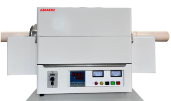
- Customer Made Versatile CVD Tube Furnace Chemical Vapor Deposition Chamber System Equipment
- Split Chamber CVD Tube Furnace with Vacuum Station Chemical Vapor Deposition System Equipment Machine
People Also Ask
- How plasma is generated in PECVD? A Step-by-Step Breakdown of the Process
- Why is PECVD better than CVD? Achieve Superior Low-Temperature Thin Film Deposition
- What is the precursor gas in PECVD? The Key to Low-Temperature Thin Film Deposition
- How is PECVD different from CVD? Unlock Low-Temperature Thin Film Deposition
- What is the difference between thermal CVD and PECVD? Choose the Right Thin-Film Deposition Method