The fundamental difference between Chemical Vapor Deposition (CVD) and Physical Vapor Deposition (PVD) lies in how a thin film is created on a substrate. PVD is a physical process that transfers a material directly onto a surface, much like spray-painting with atoms in a vacuum. In contrast, CVD is a chemical process where gas molecules react on the substrate's surface to grow an entirely new material layer.
Your choice between PVD and CVD is not about which is universally "better," but which process aligns with your specific constraints. The decision hinges on a critical trade-off: PVD offers versatility for temperature-sensitive materials through a direct physical process, while CVD provides superior, uniform coverage on complex shapes through a chemical reaction.
The Core Mechanism: Physical vs. Chemical
The names "Physical Vapor Deposition" and "Chemical Vapor Deposition" directly describe their core difference. One relies on physics, the other on chemistry.
How PVD Works: A Physical Transfer
PVD is a line-of-sight impingement process. A solid or liquid source material is converted into a vapor through physical means, such as heating it until it evaporates.
This vapor then travels in a straight line through a vacuum chamber and condenses onto the cooler substrate, forming a thin, dense film. No chemical reaction occurs.
How CVD Works: Growing from Gas
CVD involves introducing volatile precursor gases into a chamber containing the substrate.
These gases undergo chemical reactions on the heated substrate surface, decomposing and depositing the desired atoms to "grow" the film. Unwanted by-products are then removed by a continuous gas flow.
Key Differentiators in Application
The difference in mechanism leads to significant practical differences in temperature, coverage, and the types of films each method can produce.
Temperature Sensitivity
This is often the most critical deciding factor. PVD can be performed at lower substrate temperatures because it doesn't need heat to drive a chemical reaction.
This makes PVD the ideal choice for coating materials that cannot withstand the high temperatures often required for CVD processes.
Coverage and Conformality
Because PVD is a line-of-sight process, it struggles to coat complex shapes and the inside of deep holes or trenches uniformly. The material only deposits where it can "see."
CVD, however, is a multi-directional process. The precursor gases can flow around and into complex geometries, resulting in a highly uniform and conformal coating on all surfaces.
Film Properties and Quality
PVD is known for creating very dense films with fewer voids and is often used for protective coatings that require high wear resistance.
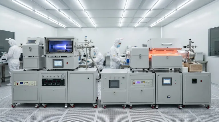
CVD is a cornerstone of the semiconductor industry for producing exceptionally high-quality, pure films, essential for applications like creating the intricate layers within CMOS technology for microprocessors and memory chips.
Understanding the Trade-offs
Choosing between these technologies requires a clear understanding of their respective costs, safety profiles, and operational complexities.
The Cost and Complexity Equation
Generally, CVD is considered a cheaper process for large-scale production, especially in established semiconductor manufacturing.
PVD is often more expensive due to the need for high-vacuum systems and more complex substrate loading and fixing procedures. It also requires skilled operators and significant cooling systems to dissipate heat from the source.
Material Handling and Safety
PVD is often considered a safer process because it does not rely on potentially toxic or corrosive precursor gases.
The chemical nature of CVD means that managing the volatile precursor gases and their by-products is a critical safety and environmental consideration.
Making the Right Choice for Your Goal
To select the correct method, you must first define your most important outcome.
- If your primary focus is coating temperature-sensitive materials: PVD is the clear choice due to its lower substrate temperature requirements.
- If your primary focus is achieving uniform coverage on complex 3D structures: CVD's multi-directional chemical deposition provides superior conformality.
- If your primary focus is cost-effective, high-quality films for CMOS manufacturing: CVD is the established and more economical industry standard for these specific processes.
- If your primary focus is a dense, wear-resistant protective coating: PVD is often preferred for its ability to form dense films with fewer voids.
Ultimately, understanding whether you need to physically "place" or chemically "grow" your thin film is the key to selecting the right deposition technology for your project.
Summary Table:
| Feature | PVD (Physical Vapor Deposition) | CVD (Chemical Vapor Deposition) |
|---|---|---|
| Core Process | Physical transfer (line-of-sight) | Chemical reaction (gas-phase) |
| Temperature | Lower substrate temperatures | Higher substrate temperatures |
| Coverage | Line-of-sight; less uniform on complex shapes | Multi-directional; highly uniform and conformal |
| Ideal For | Temperature-sensitive materials, dense protective coatings | Complex 3D structures, high-purity semiconductor films |
| Cost & Safety | Higher cost, safer (no toxic gases) | Lower cost for scale, requires gas handling |
Still unsure which deposition technology is right for your application?
At KINTEK, we specialize in providing expert guidance and high-quality lab equipment for all your thin-film deposition needs. Whether you are working with temperature-sensitive substrates or require superior conformality for complex semiconductor components, our team can help you select the ideal PVD or CVD solution.
Contact our experts today to discuss your specific requirements and discover how KINTEK's reliable equipment and consumables can enhance your laboratory's capabilities and accelerate your research and development.
Get a Personalized Consultation Now
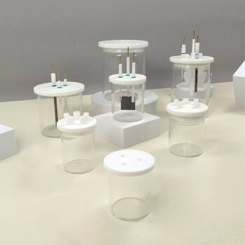
Visual Guide

Related Products
- CVD Diamond Domes for Industrial and Scientific Applications
- CVD Diamond for Thermal Management Applications
- 915MHz MPCVD Diamond Machine Microwave Plasma Chemical Vapor Deposition System Reactor
- CVD Diamond Wire Drawing Die Blanks for Precision Applications
- Customer Made Versatile CVD Tube Furnace Chemical Vapor Deposition Chamber System Equipment
People Also Ask
- What color diamonds are CVD? Understanding the Process from Brown Tint to Colorless Beauty
- Do all CVD diamonds have post growth treatment? Uncovering the Industry Standard for Gem Quality
- What is the quality of CVD diamonds? Exceptional Brilliance from a Controlled Lab Process
- Does the chemical vapor deposition be used for diamonds? Yes, for Growing High-Purity Lab Diamonds
- What is chemical vapor deposition of diamond? Grow High-Purity Diamonds Atom-by-Atom