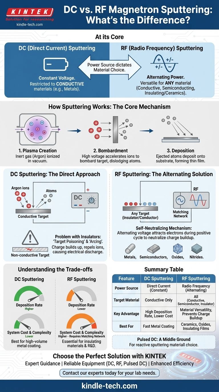
At its core, the difference between DC and RF magnetron sputtering is the type of power source used, which in turn dictates the type of material you can deposit. DC (Direct Current) sputtering uses a constant voltage and is restricted to electrically conductive target materials. RF (Radio Frequency) sputtering uses an alternating power source, making it versatile enough to deposit conductive, semiconducting, and, crucially, non-conductive (insulating) materials.
While both are powerful methods for creating high-quality thin films, the choice is dictated by your target material. DC sputtering is a fast, cost-effective method for conductive materials like metals, while RF sputtering's alternating current allows it to deposit any material, including critical insulators and ceramics.
How Sputtering Works: The Core Mechanism
A Plasma-Based Process
Magnetron sputtering is a physical vapor deposition (PVD) technique that takes place in a low-pressure vacuum chamber.
An inert gas, typically Argon, is introduced into the chamber and ionized to create a plasma—a superheated gas of ions and electrons.
Bombardment and Deposition
A high voltage is applied to the source material, known as the "target." This causes the positive ions from the plasma to accelerate and bombard the target's surface.
This bombardment dislodges, or "sputters," atoms from the target. These ejected atoms then travel through the chamber and deposit onto a substrate (the object being coated), forming a thin, dense, and highly adherent film.
The Defining Difference: Power Source and Target
DC Sputtering: The Direct Approach
DC sputtering applies a constant negative voltage to the target material. This efficiently attracts the positive Argon ions, leading to a high rate of sputtering.
This process, however, requires the target to be electrically conductive. The target must provide a path to ground for the positive charge delivered by the ions.
The "Arcing" Problem with Insulators
If you attempt to use DC sputtering on a non-conductive (insulating or dielectric) material, a problem arises. Positive charge from the Argon ions accumulates on the target's surface because there is no conductive path for it to dissipate.
This layer of positive charge, known as "target poisoning," eventually repels incoming positive ions, stopping the sputtering process. It can also lead to sudden, uncontrolled electrical discharges called arcing, which can damage the target and the power supply.
RF Sputtering: The Alternating Solution
RF sputtering solves this problem by using a high-frequency (typically 13.56 MHz) alternating current power supply. The voltage on the target rapidly oscillates between negative and positive.
During the brief positive cycle, the target attracts electrons from the plasma. These electrons neutralize the positive charge that built up on the surface during the longer, negative sputtering cycle.
The Consequence: Ultimate Material Versatility
This self-neutralizing mechanism prevents charge accumulation. As a result, RF sputtering can successfully deposit any type of material, including metals, semiconductors, and insulators like oxides and nitrides.
Understanding the Trade-offs
Deposition Rate and Efficiency
For a given conductive material, DC sputtering generally offers a higher deposition rate than RF sputtering. Its direct, continuous bombardment is more efficient, making it preferable for high-volume industrial coating of metals.
System Cost and Complexity
DC power supplies are simpler, more robust, and significantly less expensive than their RF counterparts.
RF systems require a complex and sensitive impedance matching network to ensure power is transferred efficiently from the power supply to the plasma. This adds to the overall system cost and operational complexity.
A Middle Ground: Pulsed DC Sputtering
A third option, Pulsed DC, offers a compromise. It uses a DC power source that is turned on and off in very short pulses.
The "off" time allows the charge on a less-conductive target to dissipate, mitigating arcing while often maintaining a higher deposition rate than RF. It is an excellent choice for reactive sputtering or for materials that are only semi-insulating.
Making the Right Choice for Your Goal
Ultimately, the best method depends entirely on the material you need to deposit and your production priorities.
- If your primary focus is coating with metals quickly and cost-effectively: DC sputtering is the superior choice due to its high deposition rate and lower equipment cost.
- If your primary focus is depositing insulating materials (ceramics, oxides, etc.): RF sputtering is the only viable option, as it is specifically designed to prevent the charge buildup that plagues DC systems.
- If your primary focus is research and development with diverse materials: RF sputtering provides the greatest flexibility, allowing you to experiment with any target material without changing your core equipment.
- If your primary focus is reactive sputtering or depositing semi-insulating films: Consider Pulsed DC as a high-performance alternative that balances the speed of DC with some of the material versatility of RF.
Understanding this fundamental distinction allows you to select the most efficient and effective sputtering technique for your specific material and production goals.
Summary Table:
| Feature | DC Sputtering | RF Sputtering |
|---|---|---|
| Power Source | Direct Current (Constant) | Radio Frequency (Alternating) |
| Target Material | Conductive Materials Only | All Materials (Conductive, Semiconductor, Insulator) |
| Key Advantage | High Deposition Rate, Lower Cost | Material Versatility, Prevents Charge Buildup |
| Best For | Fast, cost-effective metal coating | Depositing ceramics, oxides, and insulating films |
Choose the Perfect Sputtering Solution for Your Lab
Selecting the right sputtering technique is critical for achieving high-quality, consistent thin films. Whether your project requires the high-speed deposition of metals with DC sputtering or the versatility to coat insulating materials with RF sputtering, KINTEK has the expertise and equipment to meet your laboratory's needs.
Let KINTEK empower your research and production:
- Expert Guidance: Our specialists will help you select the ideal sputtering method for your specific materials and applications.
- Reliable Equipment: We provide robust DC, RF, and Pulsed DC sputtering systems designed for precision and durability.
- Enhanced Efficiency: Optimize your thin film deposition process to save time and reduce costs.
Ready to deposit flawless thin films? Contact our experts today to discuss your project and discover how KINTEK's lab equipment can drive your success.
Visual Guide
Related Products
- Microwave Plasma Chemical Vapor Deposition MPCVD Machine System Reactor for Lab and Diamond Growth
- Chemical Vapor Deposition CVD Equipment System Chamber Slide PECVD Tube Furnace with Liquid Gasifier PECVD Machine
- Molybdenum Tungsten Tantalum Special Shape Evaporation Boat
- Inclined Rotary Plasma Enhanced Chemical Vapor Deposition PECVD Equipment Tube Furnace Machine
- Inclined Rotary Plasma Enhanced Chemical Vapor Deposition PECVD Equipment Tube Furnace Machine
People Also Ask
- What is microwave plasma chemical vapor deposition? A Guide to High-Purity Diamond Film Growth
- How is a diamond formed from CVD? The Science of Growing Diamonds Atom by Atom
- What are the advantages of a Microwave Plasma CVD reactor for MCD/NCD coatings? Precision Multilayer Diamond Engineering
- How does MPCVD work? A Guide to Low-Temperature, High-Quality Film Deposition
- Why is argon-rich gas phase chemistry used for UNCD growth? Unlock Precision Nano-Diamond Synthesis