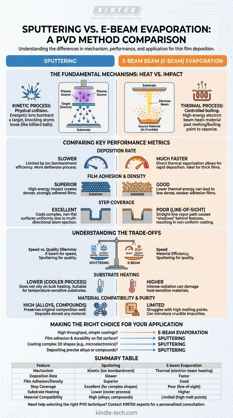
At their core, sputtering and electron beam (e-beam) evaporation are both Physical Vapor Deposition (PVD) methods, but they differ fundamentally in how they generate material vapor. E-beam evaporation uses a high-energy electron beam to boil and vaporize a source material in a crucible. In contrast, sputtering uses a physical collision, where energetic ions in a plasma bombard a target, knocking atoms loose like microscopic billiard balls.
The decision between e-beam evaporation and sputtering is a classic engineering trade-off. E-beam offers speed and material efficiency for simple geometries, while sputtering provides superior film adhesion and coverage on complex surfaces at the cost of deposition speed.
The Fundamental Mechanisms: Heat vs. Impact
To choose the right method, you must first understand the physics behind how each one creates a thin film. They operate on entirely different principles.
Electron Beam Evaporation: A Thermal Process
E-beam evaporation is essentially a highly controlled boiling process. A focused beam of electrons is directed at a source material, such as a pellet or ingot, held within a vacuum chamber.
This intense energy heats the material past its melting and boiling points, causing it to evaporate and form a vapor cloud. The substrate, positioned above the source, is then coated by this vapor as it condenses.
Sputtering: A Kinetic Process
Sputtering is a physical, non-thermal process. It begins by creating a plasma, typically from an inert gas like argon, within the vacuum chamber.
A high voltage is applied to the source material (the "target"), causing the positive argon ions from the plasma to accelerate and collide with it. This collision has enough momentum to knock out, or "sputter," atoms from the target, which then travel and deposit onto the substrate.
Comparing Key Performance Metrics
The differences in their mechanisms lead to significant differences in performance, film quality, and application suitability.
Deposition Rate
E-beam evaporation generally has a much higher deposition rate than sputtering. Because it's a direct thermal process, material can be vaporized very quickly, making it ideal for creating thick films or for high-throughput manufacturing.
Sputtering is a slower, more deliberate process. The rate is limited by the efficiency of the ion bombardment, which is typically lower than the rate of thermal evaporation.
Film Adhesion and Density
Sputtered atoms are knocked from the target with significant kinetic energy. When they arrive at the substrate, they impact with enough force to create denser, more strongly adhered films.
Vapor from e-beam evaporation travels with only thermal energy, which is much lower. This results in films that can be less dense and may have weaker adhesion compared to sputtered films.
Step Coverage
Sputtering provides superior "step coverage," which is the ability to coat complex, non-flat surfaces uniformly. Because sputtered atoms are ejected in many directions, they can coat the sides of trenches and other features.
E-beam is a "line-of-sight" technique. The vapor travels in a straight line from the source to the substrate, creating "shadows" behind any raised features and resulting in poor coverage on complex topographies.
Understanding the Trade-offs
Neither method is universally superior. Your choice involves balancing competing priorities of speed, quality, and material compatibility.
The Speed vs. Quality Dilemma
The high speed of e-beam evaporation is its primary advantage, but it comes at the cost of film quality. The lower-energy deposition can lead to more porous films with weaker adhesion.
Sputtering's slower deposition rate is often a disadvantage for throughput, but the resulting high-energy impact creates films of exceptional density, purity, and adhesion.
Substrate Heating
The intense radiation from the molten source in an e-beam system can significantly heat the substrate. This can damage heat-sensitive materials like polymers or certain electronic components.
Sputtering is a much cooler process, as it does not rely on bulk heating of the source material. This makes it far more suitable for depositing films onto temperature-sensitive substrates.
Material Compatibility and Purity
Sputtering can deposit almost any material, including alloys and compounds. It often preserves the material's original composition (stoichiometry) very well, as atoms are physically knocked loose.
E-beam evaporation can struggle with materials that have extremely high melting points or that decompose when heated. It can also introduce impurities if the electron beam inadvertently strikes the crucible holding the source material.
Making the Right Choice for Your Application
Selecting the correct technique requires a clear understanding of your project's most critical outcome.
- If your primary focus is high throughput for simple optical or metal coatings: E-beam evaporation is often the more cost-effective choice due to its high deposition rates.
- If your primary focus is film adhesion and durability on a flat surface: Sputtering is superior due to the higher energy of deposited atoms creating denser, better-adhered films.
- If your primary focus is coating complex 3D shapes like microelectronics or medical devices: Sputtering's excellent step coverage is non-negotiable for ensuring uniform coating.
- If your primary focus is depositing precise alloys or compounds without altering their composition: Sputtering provides far better control over maintaining the material's original stoichiometry.
Understanding these core principles empowers you to select the deposition technique that aligns perfectly with your material, geometry, and performance goals.
Summary Table:
| Feature | Sputtering | E-beam Evaporation |
|---|---|---|
| Mechanism | Kinetic (ion bombardment) | Thermal (electron beam heating) |
| Deposition Rate | Slower | Faster |
| Film Adhesion/Density | Superior | Good |
| Step Coverage | Excellent (for complex shapes) | Poor (line-of-sight) |
| Substrate Heating | Lower (cooler process) | Higher |
| Material Compatibility | High (alloys, compounds) | Limited (high melt points) |
Need help selecting the right PVD technique for your specific application? The choice between sputtering and e-beam evaporation is critical for achieving optimal film quality, adhesion, and throughput. KINTEK specializes in lab equipment and consumables, serving laboratory needs. Our experts can help you determine the best solution for coating complex medical devices, creating durable optical films, or depositing precise alloys. Contact our team today for a personalized consultation and elevate your thin-film deposition process!
Visual Guide