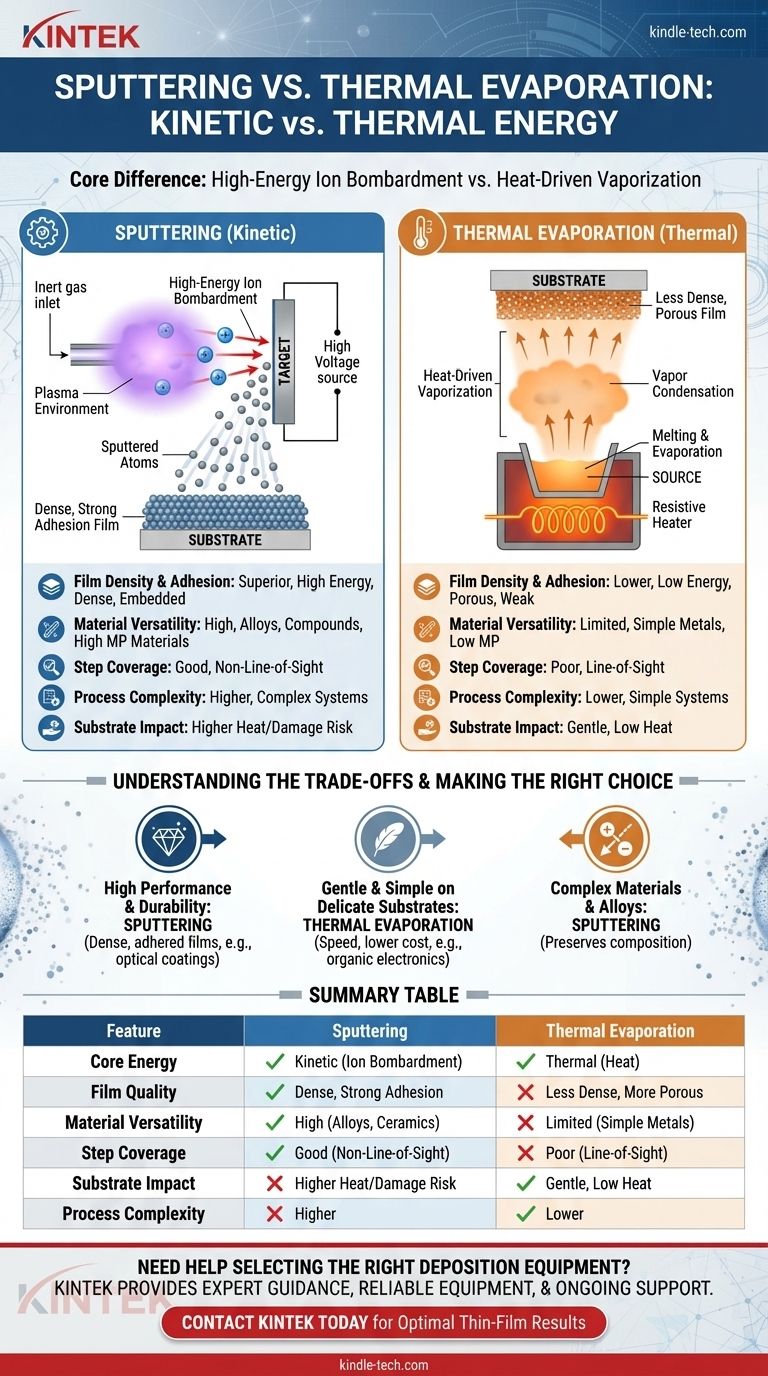
At its core, the difference between sputtering and thermal evaporation is a matter of kinetic versus thermal energy. Sputtering is a physical process that uses high-energy ion bombardment to kinetically "knock" atoms off a target material for deposition. In contrast, thermal evaporation is a simpler process that uses heat to boil a material into a vapor, which then condenses onto a substrate.
While both are methods of Physical Vapor Deposition (PVD), the choice between them comes down to a fundamental trade-off: Sputtering offers superior film quality and material versatility at the cost of complexity, whereas thermal evaporation provides simplicity and speed for a more limited range of materials.
The Core Mechanisms: Momentum vs. Heat
To understand which method suits your goal, you must first understand how each one works at an atomic level. The mechanism directly dictates the properties of the final film.
How Thermal Evaporation Works
Thermal evaporation is the more intuitive of the two processes. It is analogous to boiling water and seeing condensation form on a cool surface above the pot.
The source material is placed inside a high-vacuum chamber and heated until it melts and evaporates, creating a vapor. This vapor then travels through the vacuum and condenses as a thin film on a cooler substrate placed above it.
This method is considered a "line-of-sight" process, as the vapor travels in a relatively straight line from the source to the substrate.
How Sputtering Works
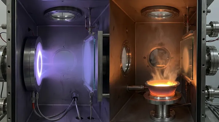
Sputtering is a kinetic process, often compared to an atomic-scale game of billiards. It does not rely on melting the source material.
First, an inert gas like argon is introduced into the vacuum chamber and energized to create a plasma. High voltage then accelerates these positively charged argon ions, causing them to collide with the source material, known as the target.
These high-energy collisions physically eject or "sputter" atoms from the target. These ejected atoms travel and deposit onto the substrate, forming a thin film.
Comparing the Resulting Film Properties
The difference in energy transfer—kinetic bombardment versus gentle condensation—has profound implications for the quality and characteristics of the deposited film.
Film Density and Adhesion
Sputtered atoms arrive at the substrate with significantly higher kinetic energy than evaporated atoms.
This high energy creates a denser, more uniform film with superior adhesion, as the atoms can physically embed themselves into the substrate's surface layer.
Evaporated films are often less dense and more porous, with weaker adhesion, because the atoms simply condense on the surface with low energy.
Material Versatility
Sputtering is exceptionally versatile. Since it is a momentum-transfer process, it can deposit virtually any material, including alloys, compounds, and high-melting-point materials like ceramics and refractory metals. The composition of the sputtered film is very close to that of the target.
Thermal evaporation is limited to materials that can be evaporated at a reasonable temperature without decomposing. It is very difficult to evaporate alloys or compounds uniformly, as the constituent elements often have different vapor pressures and evaporate at different rates.
Step Coverage
"Step coverage" refers to a film's ability to coat uneven surfaces, such as microscopic trenches on a semiconductor wafer.
Sputtering typically provides better step coverage. The sputtered atoms can scatter off gas molecules in the chamber, allowing them to coat sidewalls and other non-line-of-sight surfaces.
Thermal evaporation's line-of-sight nature results in poor step coverage, with thick films on top surfaces and very thin or non-existent films on sidewalls.
Understanding the Trade-offs
Neither method is universally superior. The choice involves balancing process complexity, cost, and potential damage to the substrate.
Process Complexity and Cost
Thermal evaporation systems are generally simpler, cheaper to build, and can achieve higher deposition rates for simple metals like aluminum or gold.
Sputtering systems are more complex and expensive. They require high-voltage power supplies, intricate gas and pressure controls, and often powerful magnets (in magnetron sputtering) to increase efficiency.
Substrate Heating and Damage
The plasma environment in sputtering generates significant heat and can cause radiation damage to the substrate. This is a critical concern for sensitive substrates like polymers or organic electronic devices (OLEDs).
Thermal evaporation is a much "gentler" process. While the source is hot, the substrate can remain near room temperature, making it ideal for depositing metals onto heat-sensitive materials.
Control and Repeatability
Sputtering offers excellent control. The deposition rate is stable and can be precisely managed by adjusting the electrical power and gas pressure, leading to highly repeatable film thickness.
Controlling the deposition rate in thermal evaporation is more difficult, as it depends on precise temperature control of the source, which can be prone to fluctuation.
Making the Right Choice for Your Goal
Your application's specific requirements for film quality, material type, and substrate sensitivity will dictate the best deposition method.
- If your primary focus is high performance and durability: Sputtering is the clear choice for creating dense, strongly adhered films like optical coatings, hard coatings on tools, or complex electronic layers.
- If your primary focus is depositing simple metals on delicate substrates: Thermal evaporation is often preferred for its gentle nature, speed, and lower cost, making it ideal for organic electronics or basic metallization.
- If your primary focus is depositing complex materials or alloys: Sputtering is the only viable PVD method, as it preserves the target's composition in the final film.
Ultimately, understanding the fundamental energy source of each process empowers you to select the tool that best achieves your desired outcome.
Summary Table:
| Feature | Sputtering | Thermal Evaporation |
|---|---|---|
| Core Energy | Kinetic (Ion Bombardment) | Thermal (Heat) |
| Film Quality | Dense, Strong Adhesion | Less Dense, More Porous |
| Material Versatility | High (Alloys, Ceramics) | Limited (Simple Metals) |
| Step Coverage | Good (Non-Line-of-Sight) | Poor (Line-of-Sight) |
| Substrate Impact | Higher Heat/Damage Risk | Gentle, Low Heat |
| Process Complexity | Higher | Lower |
Need Help Selecting the Right Deposition Equipment?
Choosing between sputtering and thermal evaporation is critical for your project's success. KINTEK specializes in providing high-quality lab equipment and consumables for all your Physical Vapor Deposition (PVD) needs. Whether you require the superior film quality of a sputtering system or the gentle, cost-effective nature of thermal evaporation for delicate substrates, our experts can help you identify the perfect solution.
We provide value by:
- Expert Guidance: Helping you select the right technology based on your material, film quality, and substrate requirements.
- Reliable Equipment: Supplying robust and precise PVD systems for consistent, repeatable results.
- Ongoing Support: Ensuring your lab operates at peak efficiency with comprehensive service and consumables.
Ready to achieve optimal thin-film results? Contact KINTEK today to discuss your specific application and find the ideal PVD solution for your laboratory.
Visual Guide