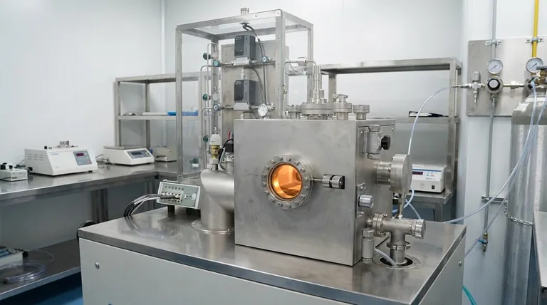
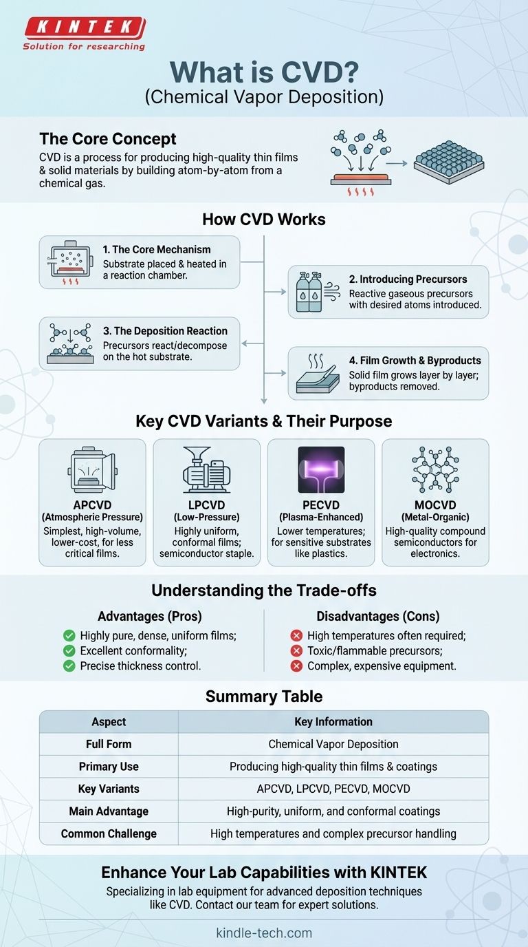
In the context of physics and materials science, CVD stands for Chemical Vapor Deposition. It is a highly versatile and widely used vacuum deposition method for producing high-quality thin films and solid materials. This process involves introducing reactive gases into a chamber, which then decompose and react on a heated substrate surface to form the desired material coating.
The core concept of CVD is not just about layering a material, but about building a new, high-purity solid layer atom-by-atom from a chemical gas. This makes it a foundational technique for manufacturing advanced electronics, optics, and protective coatings.
How Chemical Vapor Deposition Works
The CVD process, while complex in its details, follows a fundamental sequence of steps. Understanding this sequence is key to appreciating its power and its limitations.
The Core Mechanism
At its heart, CVD is a chemical process that transforms gas into a solid. A substrate, which is the material to be coated, is placed inside a reaction chamber and heated to a specific temperature.
Introducing the Precursors
Gaseous molecules called precursors, which contain the atoms of the desired film material, are then introduced into the chamber. These precursors are carefully selected for their ability to react or decompose at the substrate's temperature.
The Deposition Reaction
When the precursor gases come into contact with the hot substrate, they undergo a chemical reaction or decomposition. This reaction breaks down the precursor molecules, releasing the desired atoms which then bond to the substrate surface.
Film Growth and Byproducts
As this process continues, a thin, solid film grows layer by layer on the substrate. The other atoms from the precursor molecules, now byproducts, are removed from the chamber by a vacuum or gas flow system, leaving behind a pure and uniform coating.
Key CVD Variants and Their Purpose
Not all CVD processes are the same. Different methods have been developed to handle various materials and temperature sensitivities, each with a distinct purpose.
Atmospheric Pressure CVD (APCVD)
This is the simplest form of CVD, conducted at atmospheric pressure. It is often used for high-volume, lower-cost applications where absolute film perfection is not the primary concern.
Low-Pressure CVD (LPCVD)
By operating at sub-atmospheric pressures, LPCVD reduces unwanted gas-phase reactions. This results in highly uniform films with excellent conformity, making it a staple in semiconductor manufacturing.
Plasma-Enhanced CVD (PECVD)
PECVD uses a plasma to energize the precursor gases, allowing the deposition to occur at much lower temperatures. This is critical for coating substrates that cannot withstand the high heat required by traditional CVD methods.
Metal-Organic CVD (MOCVD)
This specialized technique uses metal-organic compounds as precursors. MOCVD is essential for creating high-quality compound semiconductor films used in advanced electronics like LEDs and high-frequency devices.
Understanding the Trade-offs
CVD is a powerful technique, but its application requires a clear understanding of its inherent advantages and disadvantages. Choosing CVD means balancing quality against complexity and cost.
Advantages of CVD
The primary strength of CVD is its ability to produce highly pure, dense, and uniform films. It offers excellent control over the film's thickness and structure. Furthermore, its ability to coat complex, non-flat surfaces (known as "conformality") is superior to many line-of-sight methods like PVD (Physical Vapor Deposition).
Common Disadvantages
The main drawbacks are the high temperatures often required, which can damage sensitive substrates, and the use of precursor gases that can be toxic, corrosive, or flammable. The equipment is also complex and expensive, and the chemical byproducts require careful handling and disposal.
Making the Right Choice for Your Application
Selecting the appropriate deposition technique depends entirely on the specific requirements of your material and end-goal.
- If your primary focus is high-purity crystalline films for semiconductors: MOCVD or LPCVD are the industry standards due to their exceptional control and uniformity.
- If your primary focus is coating temperature-sensitive materials like plastics: PECVD is the ideal choice as it allows for deposition at significantly lower temperatures.
- If your primary focus is cost-effective, large-scale production: APCVD can be a viable option when the absolute highest film quality is not a strict requirement.
Ultimately, Chemical Vapor Deposition is a cornerstone manufacturing process that enables much of modern technology by building materials from the molecule up.
Summary Table:
| Aspect | Key Information |
|---|---|
| Full Form | Chemical Vapor Deposition |
| Primary Use | Producing high-quality thin films and coatings |
| Key Variants | APCVD, LPCVD, PECVD, MOCVD |
| Main Advantage | High-purity, uniform, and conformal coatings |
| Common Challenge | High temperatures and complex precursor handling |
Ready to integrate high-purity thin films into your research or production? KINTEK specializes in lab equipment and consumables for advanced deposition techniques like CVD. Our experts can help you select the right system for your application, whether you're developing semiconductors, optics, or protective coatings. Contact our team today to discuss how our solutions can enhance your laboratory's capabilities and accelerate your project's success.
Visual Guide
Related Products
- Chemical Vapor Deposition CVD Equipment System Chamber Slide PECVD Tube Furnace with Liquid Gasifier PECVD Machine
- RF PECVD System Radio Frequency Plasma-Enhanced Chemical Vapor Deposition RF PECVD
- Microwave Plasma Chemical Vapor Deposition MPCVD Machine System Reactor for Lab and Diamond Growth
- Customer Made Versatile CVD Tube Furnace Chemical Vapor Deposition Chamber System Equipment
- 915MHz MPCVD Diamond Machine Microwave Plasma Chemical Vapor Deposition System Reactor
People Also Ask
- How expensive is chemical vapor deposition? Understanding the True Cost of High-Performance Coating
- What types of substrates are used in CVD to facilitate graphene films? Optimize Graphene Growth with the Right Catalyst
- What happens during deposition chemistry? Building Thin Films from Gaseous Precursors
- Why is Chemical Vapor Deposition (CVD) equipment uniquely suited for constructing hierarchical superhydrophobic structures?
- What is plasma enhanced chemical vapor deposition PECVD equipment? A Guide to Low-Temperature Thin Film Deposition


