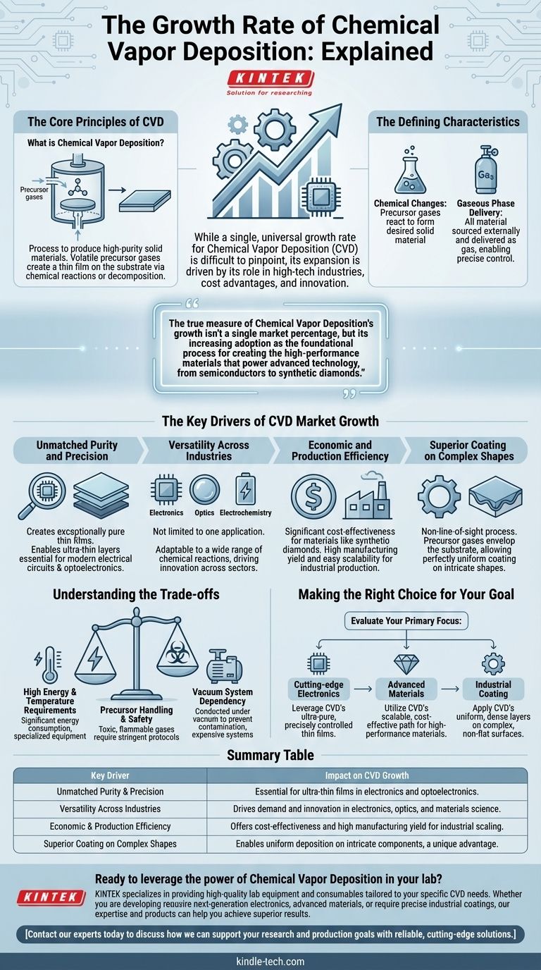
While a single, universal growth rate for Chemical Vapor Deposition (CVD) is difficult to pinpoint, the underlying drivers for its rapid expansion are clear. The technology's growth is fueled by its indispensable role in high-tech industries, significant cost advantages over traditional methods, and continuous innovation in its techniques. Its ability to produce exceptionally pure, ultra-thin material layers makes it a cornerstone of modern electronics and optics manufacturing.
The true measure of Chemical Vapor Deposition's growth isn't a single market percentage, but its increasing adoption as the foundational process for creating the high-performance materials that power advanced technology, from semiconductors to synthetic diamonds.
The Core Principles of CVD
What is Chemical Vapor Deposition?
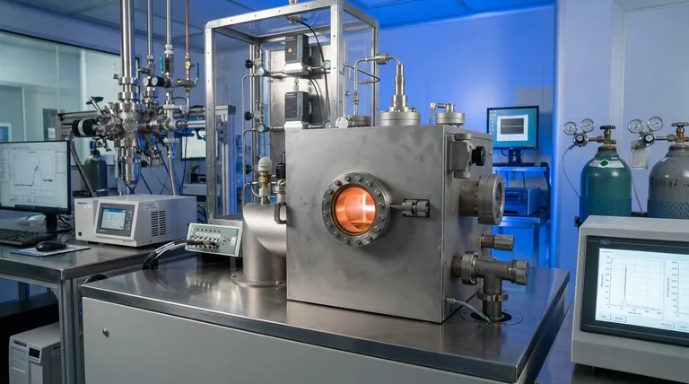
Chemical Vapor Deposition is a process used to produce high-purity, high-performance solid materials. The technique involves placing a substrate inside a reaction chamber and introducing volatile precursor gases.
Through chemical reactions or decomposition, these gases create a thin film of solid material that deposits onto the surface of the substrate.
The Defining Characteristics
Every CVD process is defined by a few key elements. First, it relies on chemical changes, where precursor gases react to form the desired solid material.
Second, all the material for the new film is sourced externally and delivered in a gaseous phase. This allows for precise control over the final product's purity and composition.
The Key Drivers of CVD Market Growth
Unmatched Purity and Precision
One of the primary advantages of CVD is its ability to create exceptionally pure thin films. The process allows for full control over timing and composition.
This precision enables the creation of ultra-thin layers of material, a non-negotiable requirement for fabricating modern electrical circuits and optoelectronic devices.
Versatility Across Industries
CVD is not limited to a single application. Its reliance on a wide range of chemical reactions makes it highly versatile.
This adaptability has unlocked new opportunities in fields like electronics, optics, and electrochemistry, driving demand and innovation across multiple sectors.
Economic and Production Efficiency
Compared to alternatives for certain materials, such as natural diamonds, CVD offers significant cost-effectiveness. This economic advantage makes high-performance materials more accessible.
Furthermore, the process boasts a high manufacturing yield and is relatively simple to scale up, making it ideal for industrial production. The deposition rates are high, and the resulting films have commendable adhesion.
Superior Coating on Complex Shapes
Unlike processes that require a direct line of sight between the source and the target, CVD is a non-line-of-sight process.
The precursor gases envelop the substrate, allowing for a perfectly uniform coating on components with complex and intricate shapes, something many other methods cannot achieve.
Understanding the Trade-offs
High Energy and Temperature Requirements
Many traditional CVD processes require very high temperatures to initiate the necessary chemical reactions. This translates to significant energy consumption and requires specialized, heat-resistant equipment.
Precursor Handling and Safety
The precursor gases used in CVD can be toxic, flammable, or corrosive. This necessitates stringent safety protocols, specialized handling equipment, and waste management systems, which can add to operational complexity and cost.
Vacuum System Dependency
A large number of CVD processes are conducted under vacuum to prevent contamination and control the reaction environment. High-quality vacuum systems can be expensive to purchase and maintain.
Making the Right Choice for Your Goal
Evaluating CVD requires aligning its core strengths with your specific objective.
- If your primary focus is cutting-edge electronics: The technology's unparalleled ability to create ultra-pure, precisely controlled thin films is its most critical advantage.
- If your primary focus is advanced materials: CVD offers a scalable and cost-effective pathway to produce high-performance materials, like synthetic diamonds, with exceptional properties.
- If your primary focus is industrial coating: The process's unique strength is its capacity to apply a uniform, dense layer of material onto complex, non-flat surfaces.
Ultimately, the sustained growth of CVD is a direct result of its fundamental ability to build materials with a level of purity and precision that modern technology demands.
Summary Table:
| Key Driver | Impact on CVD Growth |
|---|---|
| Unmatched Purity & Precision | Essential for ultra-thin films in electronics and optoelectronics. |
| Versatility Across Industries | Drives demand and innovation in electronics, optics, and materials science. |
| Economic & Production Efficiency | Offers cost-effectiveness and high manufacturing yield for industrial scaling. |
| Superior Coating on Complex Shapes | Enables uniform deposition on intricate components, a unique advantage. |
Ready to leverage the power of Chemical Vapor Deposition in your lab?
KINTEK specializes in providing high-quality lab equipment and consumables tailored to your specific CVD needs. Whether you are developing next-generation electronics, advanced materials, or require precise industrial coatings, our expertise and products can help you achieve superior results.
Contact our experts today to discuss how we can support your research and production goals with reliable, cutting-edge solutions.
Visual Guide
Related Products
- Chemical Vapor Deposition CVD Equipment System Chamber Slide PECVD Tube Furnace with Liquid Gasifier PECVD Machine
- RF PECVD System Radio Frequency Plasma-Enhanced Chemical Vapor Deposition RF PECVD
- Microwave Plasma Chemical Vapor Deposition MPCVD Machine System Reactor for Lab and Diamond Growth
- Customer Made Versatile CVD Tube Furnace Chemical Vapor Deposition Chamber System Equipment
- 915MHz MPCVD Diamond Machine Microwave Plasma Chemical Vapor Deposition System Reactor
People Also Ask
- What types of substrates are used in CVD to facilitate graphene films? Optimize Graphene Growth with the Right Catalyst
- What are the processes of vapor phase deposition? Understand CVD vs. PVD for Superior Thin Films
- What are the advantages of chemical vapor deposition? Achieve Superior Thin Films for Your Lab
- What is the chemical vapor deposition growth process? Build Superior Thin Films from the Atom Up
- What is plasma enhanced chemical vapor deposition PECVD equipment? A Guide to Low-Temperature Thin Film Deposition


