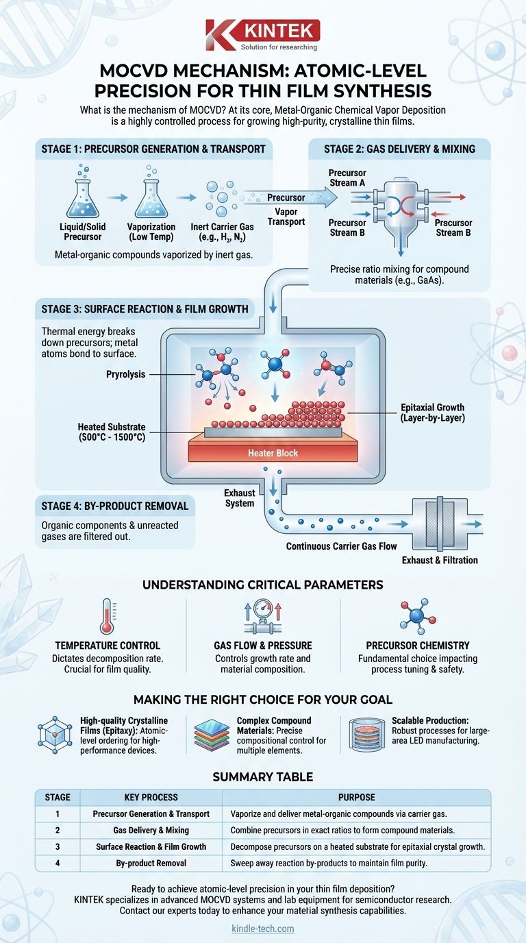
At its core, Metal-Organic Chemical Vapor Deposition (MOCVD) is a highly controlled process for growing high-purity, crystalline thin films. It works by introducing volatile metal-organic precursor gases into a reaction chamber, where they decompose on a heated substrate. This chemical reaction deposits a solid material onto the substrate surface one atomic layer at a time, resulting in a perfect or near-perfect crystal structure.
The central mechanism of MOCVD is not merely depositing material, but orchestrating a precise chemical reaction on a surface. Success hinges on manipulating gas flow, temperature, and pressure to control how precursor molecules break apart and assemble into an ordered, crystalline film.
The Four Stages of the MOCVD Process
MOCVD can be understood as a sequence of four distinct but continuous stages. This process allows for the creation of complex compound semiconductor materials essential for devices like LEDs, lasers, and high-frequency electronics.
Stage 1: Precursor Generation and Transport
The process begins with the precursors, which are specialized metal-organic compounds. These are molecules that contain the desired element (like Gallium or Aluminum) bonded to organic groups, allowing them to be vaporized at low temperatures.
To transport them, an inert carrier gas (such as hydrogen or nitrogen) is bubbled through the liquid or passed over the solid precursor. This gas picks up a precise concentration of the precursor vapor, carrying it away from the source vial and toward the reactor.
Stage 2: Gas Delivery and Mixing
The carrier gas streams, now saturated with different precursors, are routed into a gas mixing system. Here, they are combined in exact ratios.
This step is critical for creating compound materials. For example, to grow Gallium Arsenide (GaAs), streams containing a Gallium precursor and an Arsenic precursor are mixed before entering the main reaction chamber.
Stage 3: Surface Reaction and Film Growth
The mixed gases flow over a substrate (the wafer) that is heated to a high temperature, typically between 500°C and 1500°C.
This thermal energy is the catalyst for the key chemical reaction. It breaks down the precursor molecules, a process known as pyrolysis. The desired metal atoms are released and bond to the hot substrate surface.
Because of the high temperature and the pristine nature of the substrate, these atoms have enough energy to arrange themselves into the most stable configuration: a perfect crystal lattice. This layer-by-layer formation of a single crystal film is called epitaxial growth.
Stage 4: By-product Removal
The organic components of the precursor molecules, along with any unreacted gas, do not deposit onto the film. They remain in the gas phase.
The continuous flow of carrier gas acts like a current, sweeping these chemical by-products out of the reaction chamber. They are then filtered and exhausted, ensuring the growing film remains exceptionally pure.
Understanding the Critical Parameters
The quality and composition of the final film are not accidental; they are the direct result of meticulously controlling the process environment. MOCVD is less about a single setting and more about the dynamic balance of several key variables.
Temperature Control
The substrate temperature is arguably the most important parameter. It dictates the rate of the chemical decomposition reaction. If the temperature is too low, the reaction is incomplete, leading to poor film quality. If it's too high, it can cause defects or unwanted side reactions.
Gas Flow and Pressure
The flow rates of the carrier gases and the overall pressure inside the chamber determine the concentration of reactants at the substrate surface. This directly controls the growth rate of the film and the precise stoichiometry (the elemental ratio) of compound materials. Precise mass flow controllers are essential.
Precursor Chemistry
The choice of the metal-organic precursor itself is a fundamental decision. Different precursors have different vapor pressures and decomposition temperatures, requiring careful process tuning. Furthermore, these chemicals can be expensive and may have high toxicity, which impacts safety and operational costs.
Making the Right Choice for Your Goal
MOCVD is a powerful but complex technique chosen for specific, demanding applications where material quality is paramount.
- If your primary focus is high-quality crystalline films (epitaxy): MOCVD's precise control over the surface chemical reaction is what enables the atomic-level ordering required for high-performance semiconductor devices.
- If your primary focus is depositing complex compound materials: MOCVD excels at co-depositing multiple elements with exact compositional control by simply adjusting the mix of precursor gases.
- If your primary focus is scalable production: While the equipment is complex, MOCVD processes are robust and can be scaled to large-area wafers and multi-wafer systems, making it a workhorse for the industrial manufacturing of LEDs.
Ultimately, mastering MOCVD is mastering the controlled chemical synthesis of a perfect solid material directly onto a surface, one atomic layer at a time.
Summary Table:
| Stage | Key Process | Purpose |
|---|---|---|
| 1 | Precursor Generation & Transport | Vaporize and deliver metal-organic compounds via carrier gas. |
| 2 | Gas Delivery & Mixing | Combine precursors in exact ratios to form compound materials. |
| 3 | Surface Reaction & Film Growth | Decompose precursors on a heated substrate for epitaxial crystal growth. |
| 4 | By-product Removal | Sweep away reaction by-products to maintain film purity. |
Ready to achieve atomic-level precision in your thin film deposition?
KINTEK specializes in advanced lab equipment and consumables for semiconductor research and production. Our expertise in MOCVD systems can help you grow high-purity, crystalline films for LEDs, lasers, and high-frequency electronics.
Contact our experts today to discuss how we can support your laboratory's specific MOCVD needs and enhance your material synthesis capabilities.
Visual Guide
Related Products
- Multi Heating Zones CVD Tube Furnace Machine Chemical Vapor Deposition Chamber System Equipment
- 915MHz MPCVD Diamond Machine Microwave Plasma Chemical Vapor Deposition System Reactor
- Microwave Plasma Chemical Vapor Deposition MPCVD Machine System Reactor for Lab and Diamond Growth
- Cylindrical Resonator MPCVD Machine System Reactor for Microwave Plasma Chemical Vapor Deposition and Lab Diamond Growth
- Molybdenum Vacuum Heat Treat Furnace
People Also Ask
- What is the function of a tube furnace in CVD SiC synthesis? Achieving Ultra-Pure Silicon Carbide Powders
- What is the substrate for CVD process? Choosing the Right Foundation for Your Thin Film
- How does a CVD tube furnace inhibit the sintering of silver supports? Boost Membrane Durability and Performance
- What is the difference between hot wall CVD and cold wall CVD? Choose the Right System for Your Process
- What is the function of a high-temperature CVD tube furnace in 3D graphene foam prep? Master 3D Nanomaterial Growth