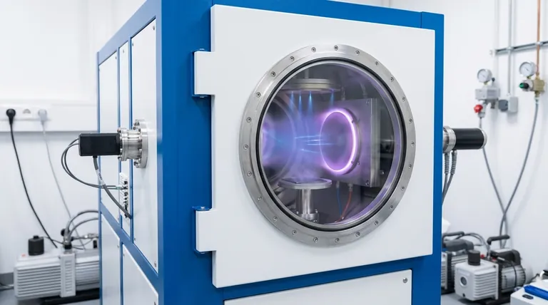
At its core, sputtering is a physical process used to create ultra-thin films of material. It works by bombarding a solid source material, known as a target, with energetic ions from a plasma. This high-energy collision physically knocks atoms loose from the target, which then travel through a vacuum and deposit onto a substrate, gradually building a uniform coating.
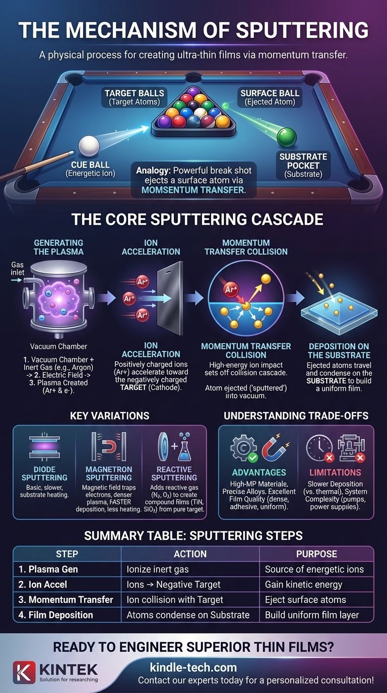
The essential mechanism of sputtering is not a chemical or thermal reaction, but a direct momentum transfer. Think of it like a powerful break shot in a game of pool: a high-energy ion (the cue ball) strikes the target (the rack of balls), causing a cascade of collisions that ejects a surface atom, which then lands precisely on your substrate.
The Core Sputtering Cascade: From Ion to Film
To understand how sputtering works, we can break it down into a sequence of four critical steps that occur inside a high-vacuum chamber.
Step 1: Generating the Plasma
First, the chamber is pumped down to a high vacuum to remove any contaminants. A small amount of an inert process gas, typically Argon (Ar), is then introduced.
An electric field is applied, which strips electrons from the argon atoms. This creates a plasma, which is an ionized gas consisting of positively charged argon ions (Ar+) and free electrons.
Step 2: Ion Acceleration and Bombardment
The target, which is the source material for the film, is given a strong negative electrical charge (making it a cathode).
The positively charged argon ions in the plasma are naturally attracted and accelerate rapidly toward this negatively charged target, gaining significant kinetic energy along the way.
Step 3: The Momentum Transfer Collision
When a high-energy argon ion collides with the target surface, it transfers its momentum to the target atoms. This initial impact sets off a chain reaction of collisions within the target material.
Eventually, an atom at the very surface of the target gains enough energy from this cascade to overcome its atomic bonds and be physically ejected, or "sputtered," into the vacuum.
Step 4: Deposition on the Substrate
The freed target atoms travel in a straight line through the vacuum until they strike a substrate (such as a silicon wafer or glass lens) that has been placed strategically in their path.
Upon arrival, these atoms condense on the substrate's surface, building up a thin, highly uniform, and dense film one atomic layer at a time.
Key Variations of the Sputtering Process
While the core principle remains the same, several methods have been developed to enhance efficiency, control, and the types of films that can be created.
Diode Sputtering
This is the most basic form of the process described above. It is effective but can have relatively low deposition rates and may cause significant heating of the substrate.
Magnetron Sputtering
This is the most common industrial method. A powerful magnetic field is placed behind the target, which traps free electrons in the plasma close to the target's surface.
This magnetic confinement dramatically increases the rate at which electrons ionize the argon gas, creating a much denser plasma. A denser plasma means more ions are available for bombardment, leading to significantly faster deposition rates and less energy wasted on heating the substrate.
Reactive Sputtering
In this technique, a reactive gas like nitrogen or oxygen is added to the inert argon gas in the chamber.
As the target metal atoms are sputtered, they chemically react with this gas on their way to the substrate. This allows for the deposition of compound films, such as hard titanium nitride (TiN) or insulating silicon dioxide (SiO₂), directly from a pure metal target.
Understanding the Trade-offs
Sputtering is an incredibly versatile and precise technique, but it comes with specific considerations that are important for any practical application.
Advantage: High-Melting-Point Materials & Alloys
Sputtering excels at depositing materials that are difficult or impossible to evaporate, such as refractory metals and complex alloys. Because the process is physical, not thermal, the original stoichiometry of an alloy target is accurately replicated in the deposited film.
Advantage: Film Quality
Sputtered films are typically dense, adhesive, and highly uniform over large areas, making the technique ideal for demanding applications in optics and electronics.
Limitation: Deposition Speed
While magnetron sputtering is very efficient, basic sputtering methods can be slow compared to other techniques like thermal evaporation. The process is best suited for creating thin films, not thick bulk coatings.
Limitation: System Complexity
Sputtering systems require expensive high-vacuum pumps, high-voltage power supplies, and precise gas flow controllers. The initial investment and operational complexity are higher than for some alternative deposition methods.
Making the Right Choice for Your Goal
Selecting the correct sputtering approach depends entirely on the desired properties of the final film.
- If your primary focus is high deposition speed for common metals: Magnetron sputtering is the industry standard for its efficiency and excellent film quality.
- If your primary focus is depositing a compound material like an oxide or nitride: Reactive sputtering is the designated method for creating these films in-situ from a pure target.
- If your primary focus is preserving the exact composition of a complex alloy: Sputtering is superior to thermal methods because it transfers the material from target to substrate without altering its chemical makeup.
- If your primary focus is coating a temperature-sensitive substrate: Magnetron sputtering is preferable as its confined plasma directs less unwanted heat onto your component.
By understanding sputtering as a controlled mechanism of atomic-scale momentum transfer, you can effectively leverage its power to engineer high-performance thin films for nearly any application.
Summary Table:
| Sputtering Step | Key Action | Purpose |
|---|---|---|
| 1. Plasma Generation | Ionize inert gas (e.g., Argon) with an electric field. | Creates a source of energetic ions for bombardment. |
| 2. Ion Acceleration | Positively charged ions accelerate toward a negatively charged target. | Gives ions the kinetic energy needed for the collision. |
| 3. Momentum Transfer | High-energy ions collide with the target, ejecting surface atoms. | Physically dislodges the material to be deposited. |
| 4. Film Deposition | Ejected atoms travel through a vacuum and condense on a substrate. | Builds a thin, uniform, and dense coating layer by layer. |
Ready to engineer superior thin films for your laboratory?
Sputtering is a powerful technique for creating high-quality, uniform coatings for applications in semiconductors, optics, and materials research. KINTEK specializes in providing advanced sputtering equipment and consumables tailored to your specific laboratory needs. Our solutions ensure precise control, reliable performance, and exceptional film quality for your most demanding projects.
Let's discuss how our sputtering systems can enhance your research and development. Contact our experts today for a personalized consultation!
Visual Guide
Related Products
- Spark Plasma Sintering Furnace SPS Furnace
- Vacuum Induction Melting Spinning System Arc Melting Furnace
- Chemical Vapor Deposition CVD Equipment System Chamber Slide PECVD Tube Furnace with Liquid Gasifier PECVD Machine
- Customer Made Versatile CVD Tube Furnace Chemical Vapor Deposition Chamber System Equipment
- Vacuum Cold Mounting Machine for Sample Preparation
People Also Ask
- What is the mechanism of SPS process? A Deep Dive into Rapid, Low-Temperature Sintering
- What are the fundamentals of spark plasma sintering process? Unlock Rapid, High-Performance Material Consolidation
- What is the theory of spark plasma sintering? A Guide to Rapid, Low-Temperature Densification
- What is the process fundamentals of spark plasma sintering? Achieve Rapid, High-Density Material Consolidation
- Why are Spark Plasma Sintering (SPS) furnaces or hot presses utilized in the preparation of Li3PS4 solid electrolytes?


